96
CY7C194
CY7C195
CY7C196
64K x 4 Static RAM
Features
鈥?High speed
鈥?12 ns
鈥?Output enable (OE) feature (7C195 and 7C196)
鈥?CMOS for optimum speed/power
鈥?Low active power
鈥?880 mW
鈥?Low standby power
鈥?220 mW
鈥?TTL-compatible inputs and outputs
鈥?Automatic power-down when deselected
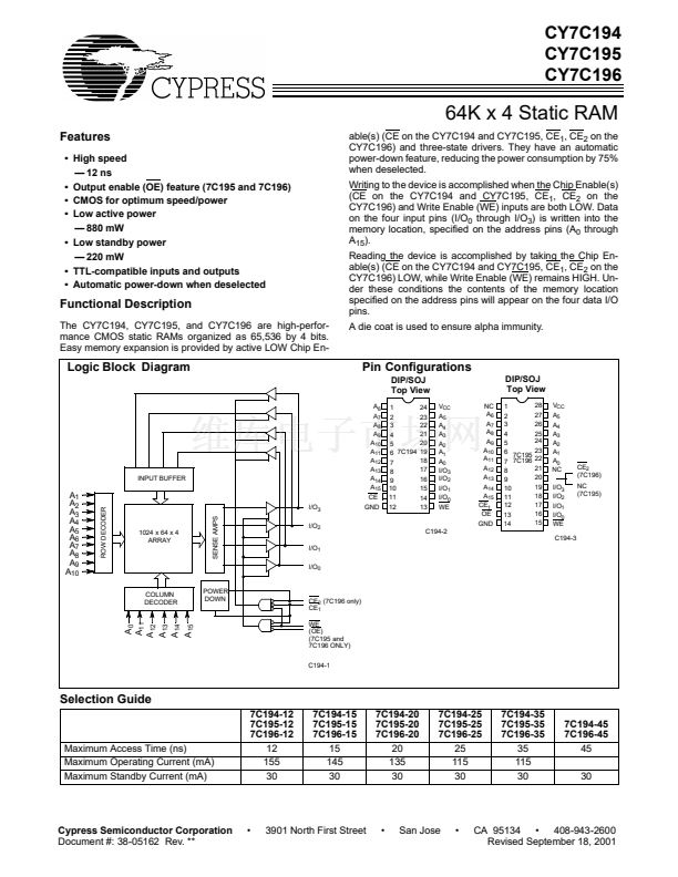
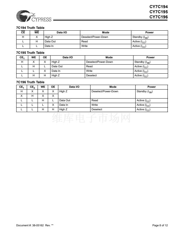
able(s) (CE on the CY7C194 and CY7C195, CE
1
, CE
2
on the
CY7C196) and three-state drivers. They have an automatic
power-down feature, reducing the power consumption by 75%
when deselected.
Writing to the device is accomplished when the Chip Enable(s)
(CE on the CY7C194 and CY7C195, CE
1
, CE
2
on the
CY7C196) and Write Enable (WE) inputs are both LOW. Data
on the four input pins (I/O
0
through I/O
3
) is written into the
memory location, specified on the address pins (A
0
through
A
15
).
Reading the device is accomplished by taking the Chip En-
able(s) (CE on the CY7C194 and CY7C195, CE
1
, CE
2
on the
CY7C196) LOW, while Write Enable (WE) remains HIGH. Un-
der these conditions the contents of the memory location
specified on the address pins will appear on the four data I/O
pins.
A die coat is used to ensure alpha immunity.
Functional Description
The CY7C194, CY7C195, and CY7C196 are high-perfor-
mance CMOS static RAMs organized as 65,536 by 4 bits.
Easy memory expansion is provided by active LOW Chip En-
Logic Block Diagram
Pin Configurations
DIP/SOJ
Top View
A
6
A
7
A
8
A
9
A
10
A
11
A
12
A
13
A
14
A
15
I/O
3
SENSE AMPS
I/O
2
I/O
1
I/O
0
CE
GND
1
2
3
4
5
6 7C194
7
8
9
10
11
12
24
23
22
21
20
19
18
17
16
15
14
13
V
CC
A
5
A
4
A
3
A
2
A
1
A
0
I/O
3
I/O
2
I/O
1
I/O
0
WE
NC
A
6
A
7
A
8
A
9
A
10
A
11
A
12
A
13
A
14
A
15
CE
1
OE
GND
DIP/SOJ
Top View
1
2
3
4
5
6 7C195
7 7C196
8
9
10
11
12
13
14
28
27
26
25
24
23
22
21
20
19
18
17
16
15
V
CC
A
5
A
4
A
3
A
2
A
1
A
0
NC
I/O
3
I/O
2
I/O
1
I/O
0
WE
C194-3
INPUT BUFFER
CE
2
(7C196)
NC
(7C195)
A
1
A
2
A
3
A
4
A
5
A
6
A
7
A
8
A
9
A
10
ROW DECODER
1024 x 64 x 4
ARRAY
C194-2
COLUMN
DECODER
POWER
DOWN
CE
2
(7C196 only)
CE
1
WE
(OE)
(7C195 and
7C196 ONLY)
C194-1
A
0
A
11
A
12
A
13
A
14
Selection Guide
7C194-12
7C195-12
7C196-12
12
155
30
7C194-15
7C195-15
7C196-15
15
145
30
7C194-20
7C195-20
7C196-20
20
135
30
7C194-25
7C195-25
7C196-25
25
115
30
7C194-35
7C195-35
7C196-35
35
115
30
7C194-45
7C196-45
45
30
Maximum Access Time (ns)
Maximum Operating Current (mA)
Maximum Standby Current (mA)
Cypress Semiconductor Corporation
Document #: 38-05162 Rev. **
A
15
鈥?/div>
3901 North First Street
鈥?/div>
San Jose
鈥?/div>
CA 95134 鈥?408-943-2600
Revised September 18, 2001


 1
1
 2
2
 3
3
 4
4
 5
5
 6
6
 7
7
 8
8
 9
9
 10
10
 11
11
 12
12
