PN200 / MMBT200 / PN200A / MMBT200A
Discrete POWER & Signal
Technologies
PN200
PN200A
MMBT200
MMBT200A
C
E
C
B
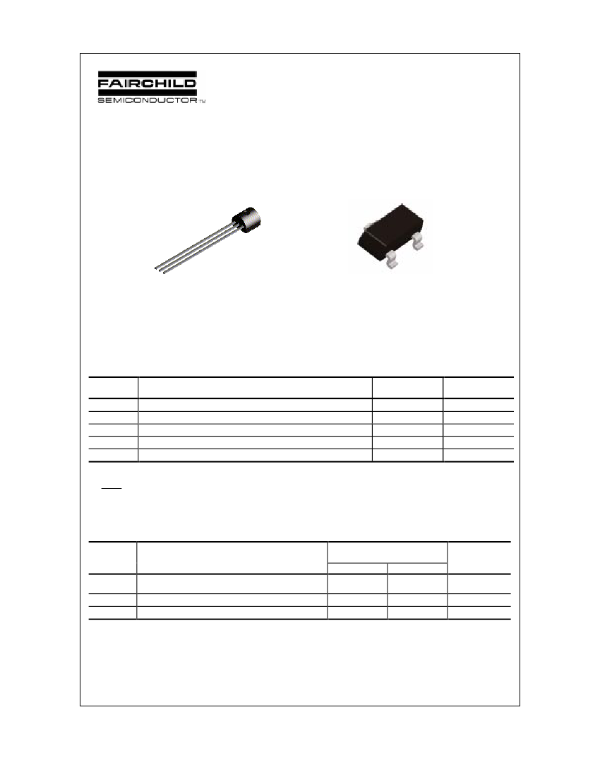
TO-92
E
SOT-23
Mark: N2 / N2A
B
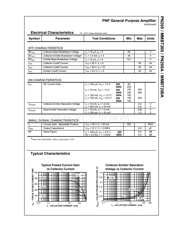
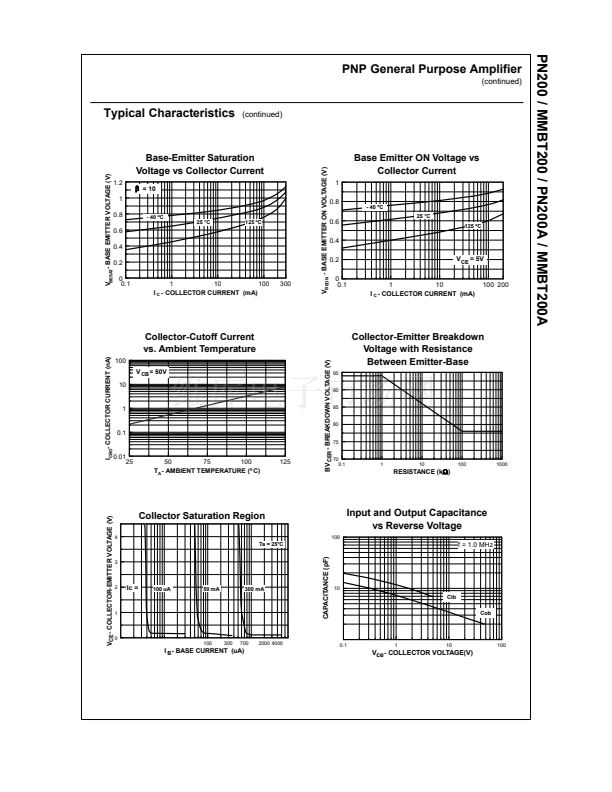
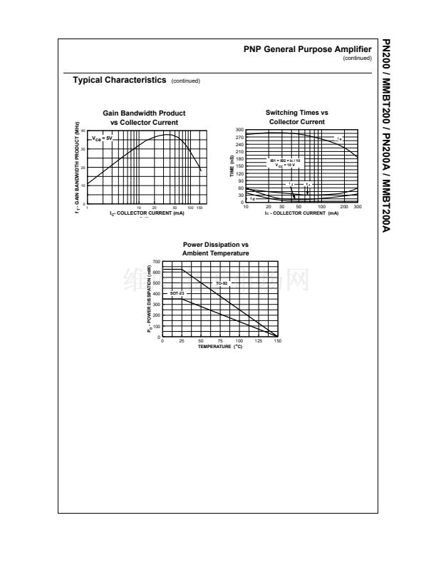
PNP General Purpose Amplifier
This device is designed for general purpose amplifier applications
at collector currents to 300 mA. Sourced from Process 68.
Absolute Maximum Ratings*
Symbol
V
CEO
V
CBO
V
EBO
I
C
T
J
, T
stg
Collector-Base Voltage
Emitter-Base Voltage
Collector Current - Continuous
TA = 25掳C unless otherwise noted
Parameter
Collector-Emitter Voltage
Value
45
75
6.0
500
-55 to +150
Units
V
V
V
mA
掳C
Operating and Storage Junction Temperature Range
*
These ratings are limiting values above which the serviceability of any semiconductor device may be impaired.
NOTES:
1)
These ratings are based on a maximum junction temperature of 150 degrees C.
2)
These are steady state limits. The factory should be consulted on applications involving pulsed or low duty cycle operations.
Thermal Characteristics
Symbol
P
D
R
胃JC
R
胃JA
TA = 25掳C unless otherwise noted
Characteristic
Total Device Dissipation
Derate above 25掳C
Thermal Resistance, Junction to Case
Thermal Resistance, Junction to Ambient
PN200A
625
5.0
83.3
200
Max
*MMBT200A
350
2.8
357
Units
mW
mW/掳C
掳C/W
掳C/W
*
Device mounted on FR-4 PCB 1.6" X 1.6" X 0.06."
漏
1997 Fairchild Semiconductor Corporation


 1
1
 2
2
 3
3
 4
4
