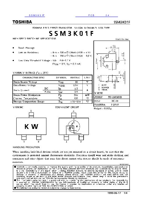
鈥?/div>
Small package
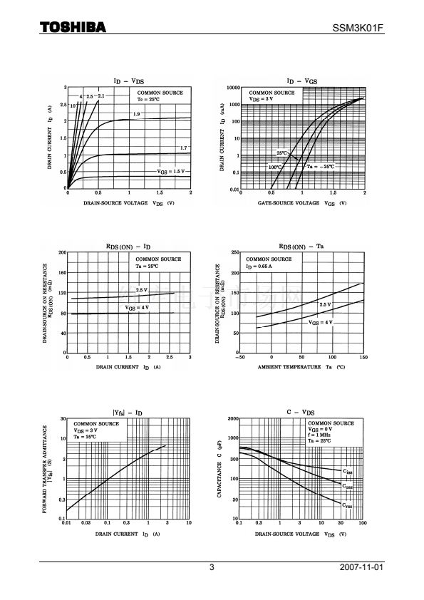
Low on resistance : Ron = 120 m鈩?(max) (V
GS
= 4 V)
: Ron = 150 m鈩?(max) (V
GS
= 2.5 V)
Low gate threshold voltage: V
th
= 0.6~1.1 V (V
DS
= 3 V, I
D
= 0.1 mA)
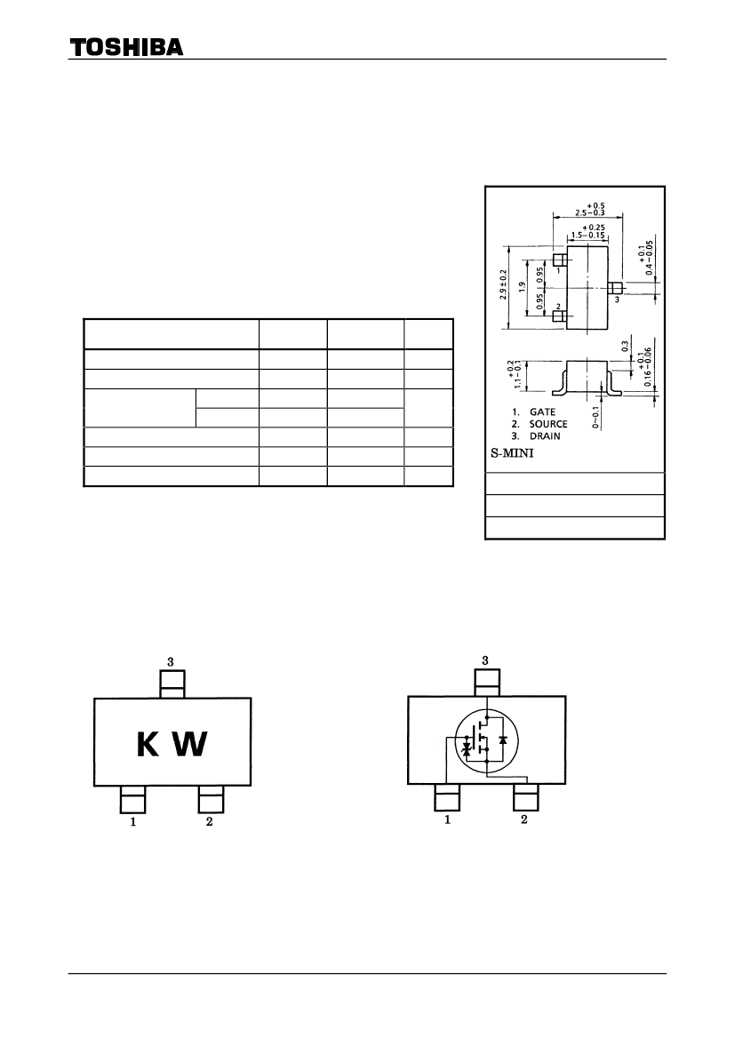
Unit: mm
Absolute Maximum Ratings
(Ta
=
25掳C)
Characteristics
Drain-source voltage
Gate-source voltage
Drain current
Drain power dissipation
Channel temperature
Storage temperature range
DC
Pulse
Symbol
V
DS
V
GSS
I
D
I
DP
P
D
T
ch
T
stg
Rating
30
卤10
1.3
2.6
200
150
鈭?5~150
Unit
V
V
A
mW
掳C
掳C
Note:
JEDEC
TO-236MOD
Using continuously under heavy loads (e.g. the application of
JEITA
SC-59
high temperature/current/voltage and the significant change in
temperature, etc.) may cause this product to decrease in the
TOSHIBA
2-3F1F
reliability significantly even if the operating conditions (i.e.
operating temperature/current/voltage, etc.) are within the
Weight: 0.012 g (typ.)
absolute maximum ratings.
Please design the appropriate reliability upon reviewing the Toshiba Semiconductor Reliability Handbook
(鈥淗andling Precautions鈥?鈥淒erating Concept and Methods鈥? and individual reliability data (i.e. reliability test
report and estimated failure rate, etc).
Marking
Equivalent Circuit
Handling Precaution
When handling individual devices (which are not yet mounted on a circuit board), be sure that the environment
is protected against electrostatic electricity. Operators should wear anti-static clothing, and containers and other
objects that come into direct contact with devices should be made of anti-static materials.
1
2007-11-01


 1
1
 2
2
 3
3
 4
4
 5
5
