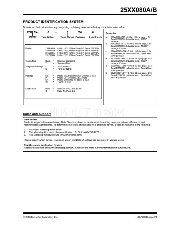
鈥?/div>
Max. clock 10 MHz
Low-power CMOS technology
1024 x 8-bit organization
16 byte page (鈥楢鈥?version devices)
32 byte page (鈥楤鈥?version devices)
Write cycle time: 5 ms max.
Self-timed ERASE and WRITE cycles
Block write protection
- Protect none, 1/4, 1/2 or all of array
Built-in write protection
- Power-on/off data protection circuitry
- Write enable latch
- Write-protect pin
Sequential read
High reliability
- Endurance: 1,000,000 erase/write cycles
- Data retention: > 200 years
- ESD protection: > 4000V
Temperature ranges supported;
- Industrial (I):
-40掳C to +85掳C
- Automotive (E):
-40掳C to +125掳C
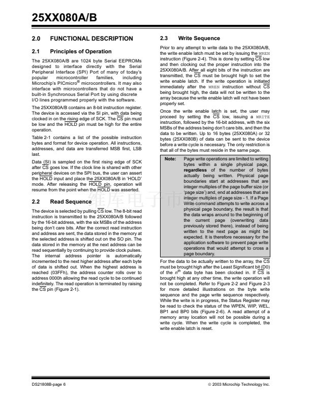
Description
The Microchip Technology Inc. 25AA080A/B,
25LC080A/B (25XX080A/B
*
) are 8 Kbit Serial
Electrically Erasable PROMs. The memory is accessed
via a simple Serial Peripheral Interface鈩?(SPI鈩?
compatible serial bus. The bus signals required are a
clock input (SCK) plus separate data in (SI) and data
out (SO) lines. Access to the device is controlled
through a Chip Select (CS) input.
Communication to the device can be paused via the
hold pin (HOLD). While the device is paused, transi-
tions on its inputs will be ignored, with the exception of
chip select, allowing the host to service higher priority
interrupts.
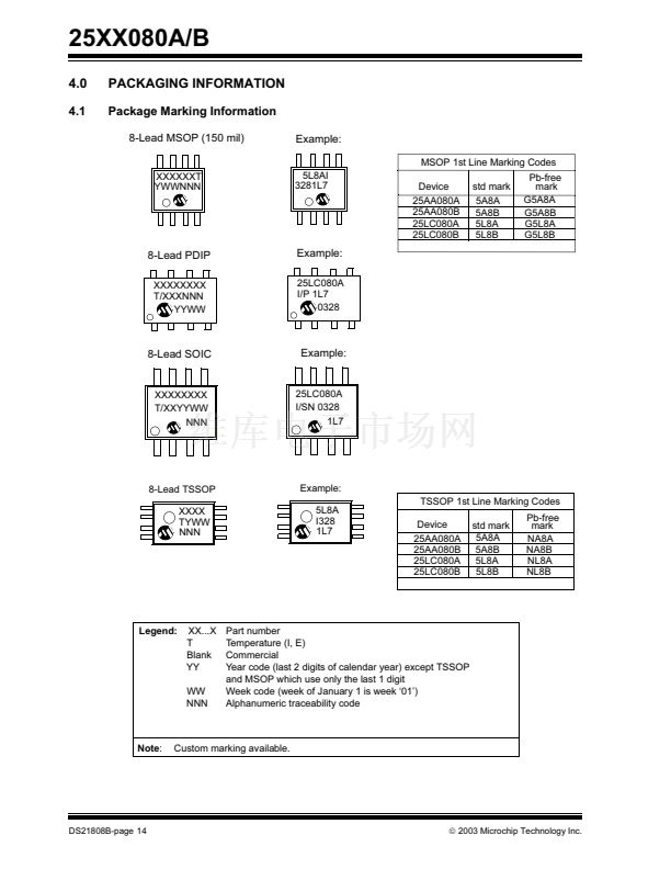
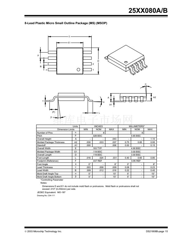
The 25XX080A/B is available in standard packages
including 8-lead PDIP and SOIC, and advanced
packaging including 8-lead MSOP, and 8-lead TSSOP.
Pb-free (Pure Matte Sn) finish is also available.
鈥?/div>
鈥?/div>
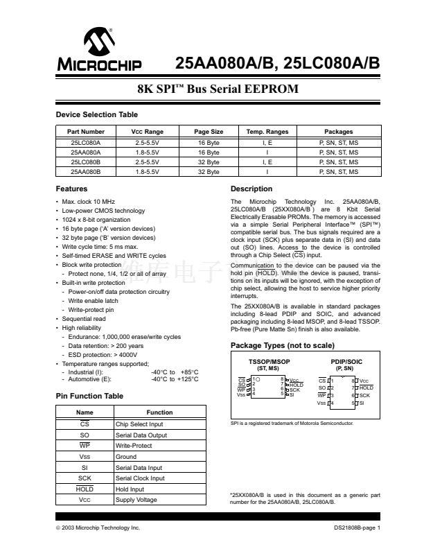
Package Types (not to scale)
TSSOP/MSOP
(ST, MS)
CS
SO
WP
V
SS
1
2
3
4
8
7
6
5
V
CC
HOLD
SCK
SI
鈥?/div>
PDIP/SOIC
(P, SN)
CS
SO
WP
V
SS
1
2
3
4
8
7
6
5
V
CC
HOLD
SCK
SI
Pin Function Table
Name
CS
SO
WP
V
SS
SI
SCK
HOLD
V
CC
Function
Chip Select Input
Serial Data Output
Write-Protect
Ground
Serial Data Input
Serial Clock Input
Hold Input
Supply Voltage
SPI is a registered trademark of Motorola Semiconductor.
*25XX080A/B is used in this document as a generic part
number for the 25AA080A/B, 25LC080A/B.
铮?/div>
2003 Microchip Technology Inc.
DS21808B-page 1


 1
1
 2
2
 3
3
 4
4
 5
5
 6
6
 7
7
 8
8
 9
9
 10
10
 11
11
 12
12
 13
13
 14
14
 15
15
 16
16
 17
17
 18
18
 19
19
 20
20
 21
21
 22
22
 23
23
 24
24
