鈥?/div>
Pb鈭扚ree Packages are Available*
http://onsemi.com
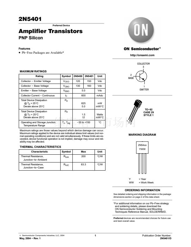
COLLECTOR
3
MAXIMUM RATINGS
Rating
Collector 鈭?Emitter Voltage
Collector 鈭?Base Voltage
Emitter 鈭?Base Voltage
Collector Current 鈭?Continuous
Total Device Dissipation
@ T
A
= 25掳C
Derate above 25掳C
Total Device Dissipation
@ T
C
= 25掳C
Derate above 25掳C
Operating and Storage Junction
Temperature Range
Symbol
V
CEO
V
CBO
V
EBO
I
C
P
D
625
5.0
P
D
1.5
12
T
J
, T
stg
鈭?5 to +150
Watts
mW/掳C
掳C
12
3
mW
mW/掳C
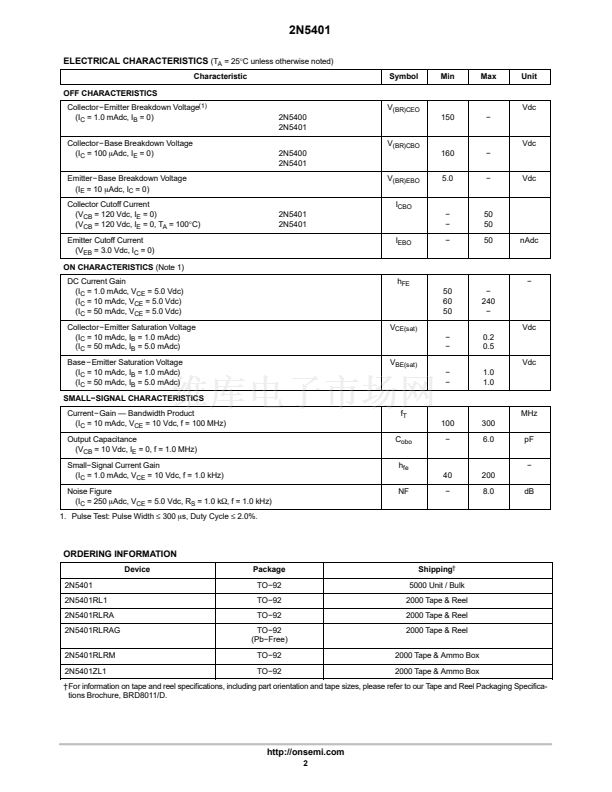
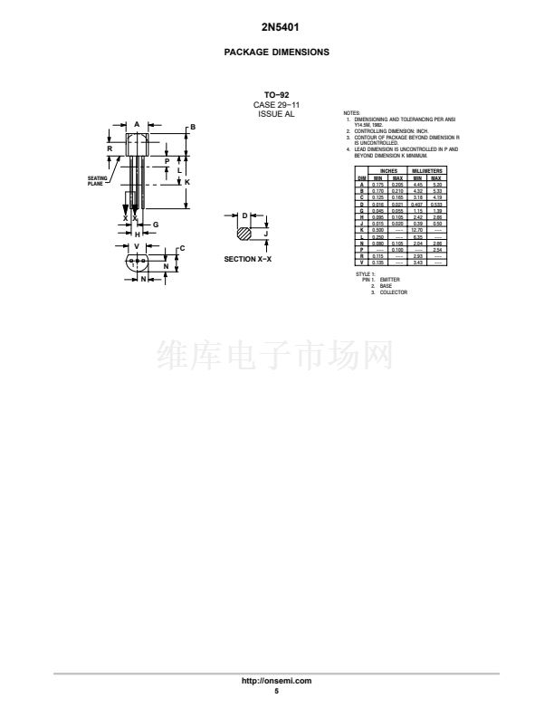
TO鈭?2
CASE 29
STYLE 1
2N5400 2N5401
120
130
5.0
600
150
160
Unit
Vdc
Vdc
Vdc
mAdc
1
EMITTER
2
BASE
Maximum ratings are those values beyond which device damage can occur.
Maximum ratings applied to the device are individual stress limit values (not nor-
mal operating conditions) and are not valid simultaneously. If these limits are ex-
ceeded, device functional operation is not implied, damage may occur and reli-
ability may be affected.
MARKING DIAGRAM
THERMAL CHARACTERISTICS
Characteristic
Thermal Resistance,
Junction鈭抰o鈭扐mbient
Thermal Resistance,
Junction鈭抰o鈭扖ase
Symbol
R
qJA
R
qJC
Max
200
83.3
Unit
掳C/W
掳C/W
2N54xx
YWW
Y
WW
= Year
= Work Week
ORDERING INFORMATION
See detailed ordering and shipping information in the package
dimensions section on page 2 of this data sheet.
*For additional information on our Pb鈭扚ree strategy
and soldering details, please download the
ON Semiconductor Soldering and Mounting
Techniques Reference Manual, SOLDERRM/D.
Preferred
devices are recommended choices for future use
and best overall value.
漏
Semiconductor Components Industries, LLC, 2004
1
May, 2004 鈭?Rev. 1
Publication Order Number:
2N5401/D


 1
1
 2
2
 3
3
 4
4
 5
5
 6
6
