0.65 max.
max.
鈭?/div>
0.05
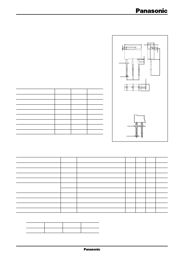
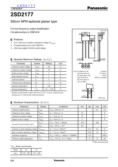
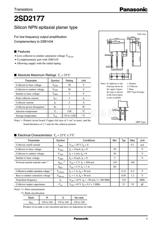
Note) In addition to the
lead type shown in
the upper figure,
the type as shown
in the lower figure
is also available.
1: Emitter
2: Collector
3: Base
MT2 Type Package
Note) *: Printed circuit board: Copper foil area of 1
or more, and the
board thickness of 1.7 mm for the collector portion
2.5卤0.1
I
Absolute Maximum Ratings
T
a
=
25掳C
1
2
3
0.45
鈭?.05
+0.1
2.5卤0.5
2.5卤0.5
(HW Type)
I
Electrical Characteristics
T
a
=
25掳C
卤
3掳C
Parameter
Collector cutoff current
Collector to base voltage
Collector to emitter voltage
Emitter to base voltage
Forward current transfer ratio
*1
Symbol
I
CBO
V
CBO
V
CEO
V
EBO
h
FE1
h
FE2
*2
Conditions
V
CB
=
20 V, I
E
=
0
I
C
=
10
碌A,
I
E
=
0
I
C
=
1 mA, I
B
=
0
I
E
=
10
碌A,
I
C
=
0
V
CE
=
2 V, I
C
=
200 mA
V
CE
=
2 V, I
C
=
1 A
I
C
=
1 A, I
B
=
50 mA
I
C
=
1 A, I
B
=
50 mA
V
CB
=
10 V, I
E
= 鈭?0
mA, f
=
200 MHz
V
CB
=
10 V, I
E
= 0,
f
=
1 MHz
Min
Typ
Max
0.1
14.5卤0.5
0.5
4.5卤0.1
Unit
碌A
V
V
V
50
50
5
120
80
0.15
0.85
110
23
35
0.3
1.2
340
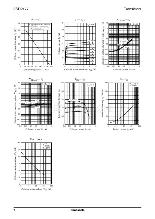
Collector to emitter saturation voltage
*1
Base to emitter saturation voltage
*1
Transition frequency
Collector output capacitance
Note) *1: Pulse measurement
*2: Rank classification
Rank
h
FE1
R
120 to 240
V
CE(sat)
V
BE(sat)
f
T
C
ob
V
V
MHz
pF
S
170 to 340
No-rank
120 to 340
Product of no-rank is not classified and have no indication for rank.
1


 1
1
 2
2
