鈥?/div>
Low drain-source ON resistance: R
DS (ON)
= 65 m鈩?(typ.)
High forward transfer admittance: |Y
fs
| = 10 S (typ.)
Low leakage current: I
DSS
= 100 碌A (V
DS
= 200 V)
Enhancement mode: V
th
= 3.0 to 5.0 V (V
DS
= 10 V, I
D
= 1 mA)
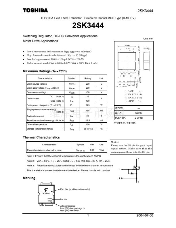
Unit: mm
Maximum Ratings
(Ta
=
25掳C)
Characteristics
Drain-source voltage
Drain-gate voltage (R
GS
=
20 k鈩?
Gate-source voltage
Drain current
DC
(Note 1)
Symbol
V
DSS
V
DGR
V
GSS
I
D
I
DP
P
D
E
AS
I
AR
E
AR
T
ch
T
stg
Rating
200
200
卤30
25
100
125
488
25
12.5
150
鈭?5
to 150
Unit
V
V
V
A
W
mJ
A
mJ
掳C
掳C
Pulse (Note 1)
Drain power dissipation (Tc
=
25掳C)
Single pulse avalanche energy
(Note 2)
Avalanche current
Repetitive avalanche energy (Note 3)
Channel temperature
Storage temperature range
JEDEC
JEITA
TOSHIBA
鈥?/div>
SC-97
2-9F1B
Weight: 0.74 g (typ.)
Thermal Characteristics
Characteristics
Thermal resistance, channel to case
Symbol
R
th (ch-c)
Max
1.00
Unit
掳C/W
Notice:
Please use the S1 pin for gate input
signal return. Make sure that the
main current flows into the S2 pin.
4
Note 1: Ensure that the channel temperature does not exceed 150掳C.
Note 2: V
DD
=
50 V, T
ch
=
25掳C (initial), L
=
1.26 mH, I
AR
=
25 A, R
G
=
25
鈩?/div>
Note 3: Repetitive rating: pulse width limited by maximum channel temperature
This transistor is an electrostatic-sensitive device. Please handle with caution.
1
Marking
2
3
Part No. (or abbreviation code)
K3444
Lot No.
A line indicates
lead (Pb)-free package or
lead (Pb)-free finish.
1
2004-07-06


 1
1
 2
2
 3
3
 4
4
 5
5
 6
6
