74F74 Dual D-Type Positive Edge-Triggered Flip-Flop
April 1988
Revised September 2000
74F74
Dual D-Type Positive Edge-Triggered Flip-Flop
General Description
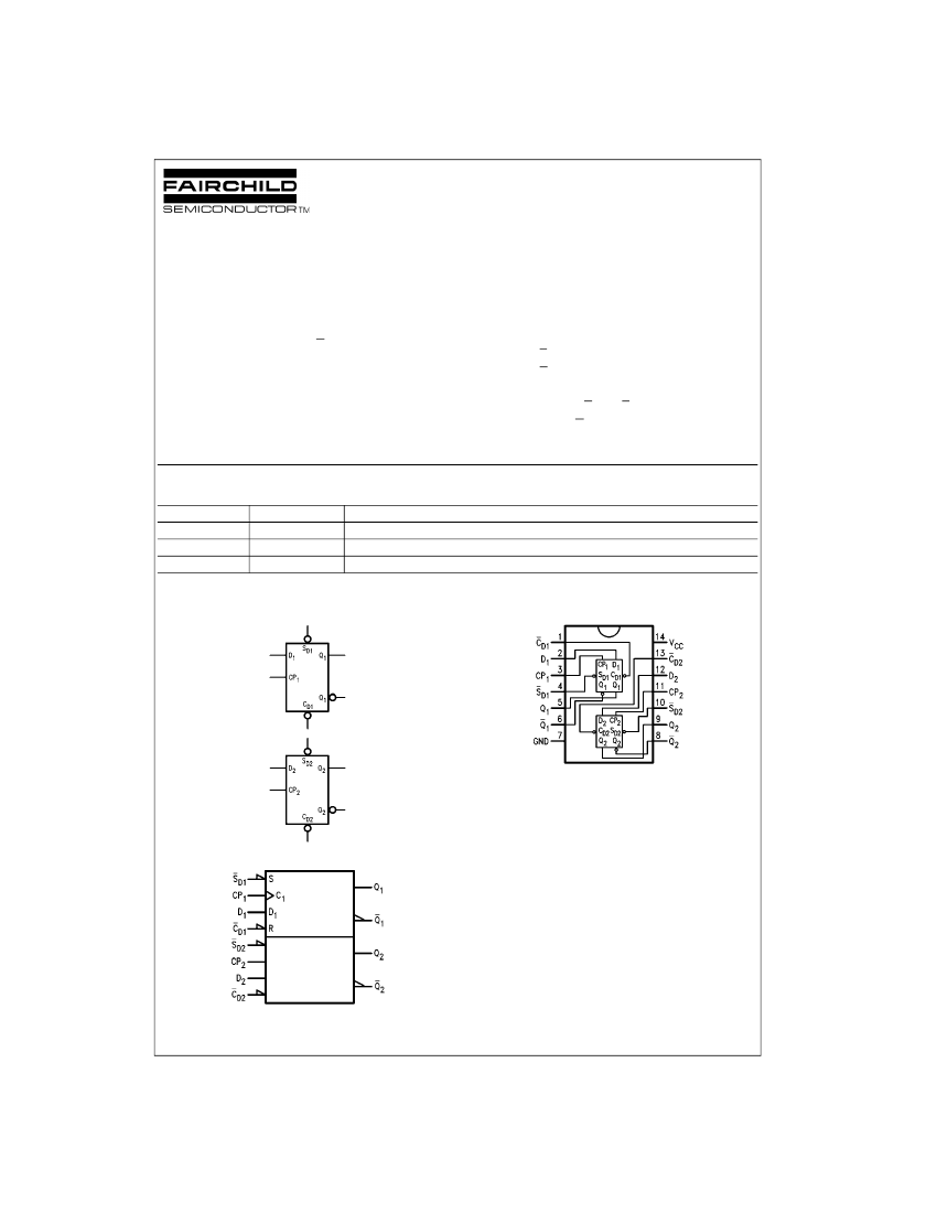
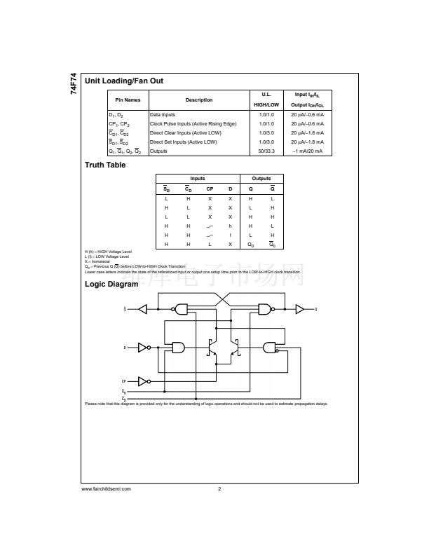
The F74 is a dual D-type flip-flop with Direct Clear and Set
inputs and complementary (Q, Q) outputs. Information at
the input is transferred to the outputs on the positive edge
of the clock pulse. Clock triggering occurs at a voltage level
of the clock pulse and is not directly related to the transition
time of the positive-going pulse. After the Clock Pulse input
threshold voltage has been passed, the Data input is
locked out and information present will not be transferred to
the outputs until the next rising edge of the Clock Pulse
input.
Asynchronous Inputs:
LOW input to S
D
sets Q to HIGH level
LOW input to C
D
sets Q to LOW level
Clear and Set are independent of clock
Simultaneous LOW on C
D
and S
D
makes both Q and Q HIGH
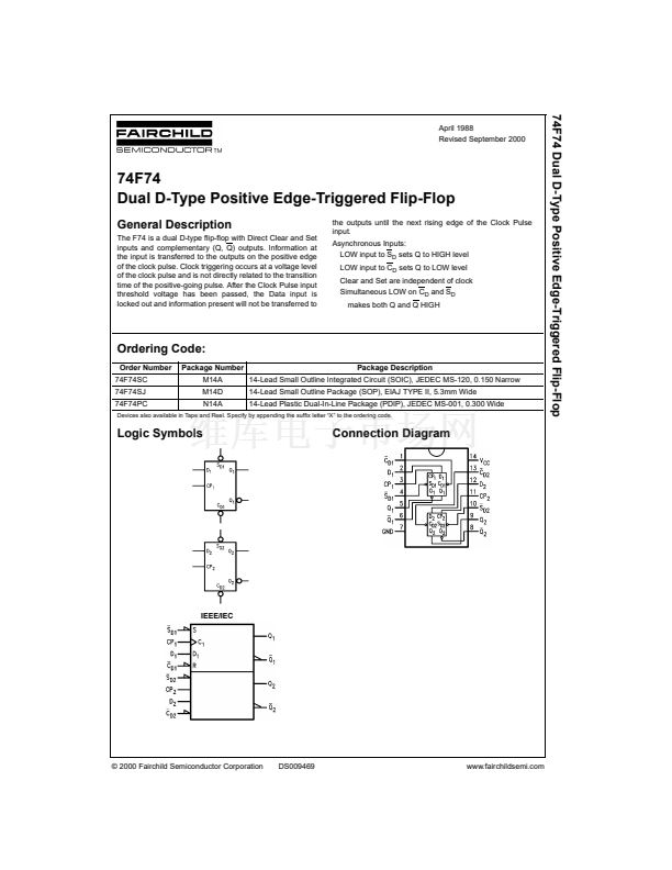
Ordering Code:
Order Number
74F74SC
74F74SJ
74F74PC
Package Number
M14A
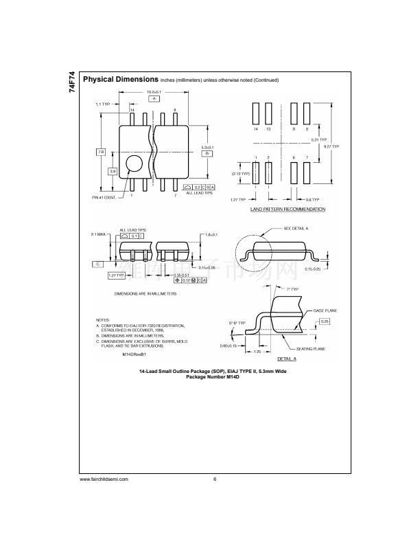
M14D
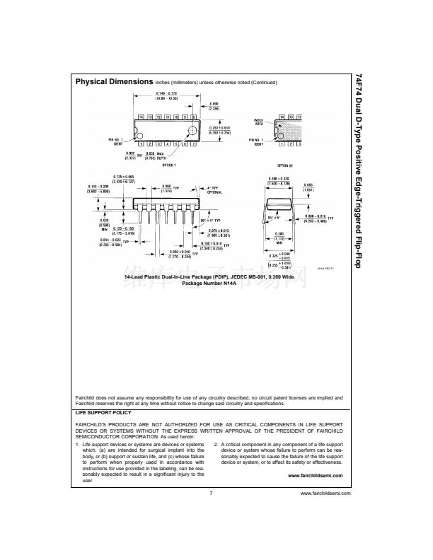
N14A
Package Description
14-Lead Small Outline Integrated Circuit (SOIC), JEDEC MS-120, 0.150 Narrow
14-Lead Small Outline Package (SOP), EIAJ TYPE II, 5.3mm Wide
14-Lead Plastic Dual-In-Line Package (PDIP), JEDEC MS-001, 0.300 Wide
Devices also available in Tape and Reel. Specify by appending the suffix letter 鈥淴鈥?to the ordering code.
Logic Symbols
Connection Diagram
IEEE/IEC
漏 2000 Fairchild Semiconductor Corporation
DS009469
www.fairchildsemi.com


 1
1
 2
2
 3
3
 4
4
 5
5
 6
6
 7
7
