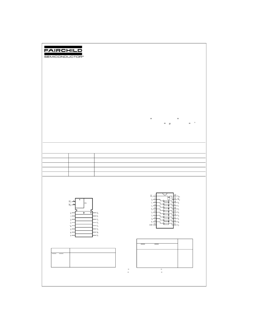
74VHCT541A Octal Buffer/Line Driver with 3-STATE Outputs
June 1997
Revised April 2005
74VHCT541A
Octal Buffer/Line Driver with 3-STATE Outputs
General Description
The VHCT541A is an advanced high-speed CMOS device
fabricated with silicon gate CMOS technology. It achieves
the high-speed operation similar to equivalent Bipolar
Schottky TTL while maintaining the CMOS low power dissi-
pation.
The VHCT541A is an octal buffer/line driver designed to be
employed as memory and address drivers, clock drivers
and bus oriented transmitter/receivers.
This device is similar in function to the VHCT244A while
providing flow-through architecture (inputs on opposite side
from outputs). This pinout arrangement makes this device
especially useful as an output port for microprocessors,
allowing ease of layout and greater PC board density.
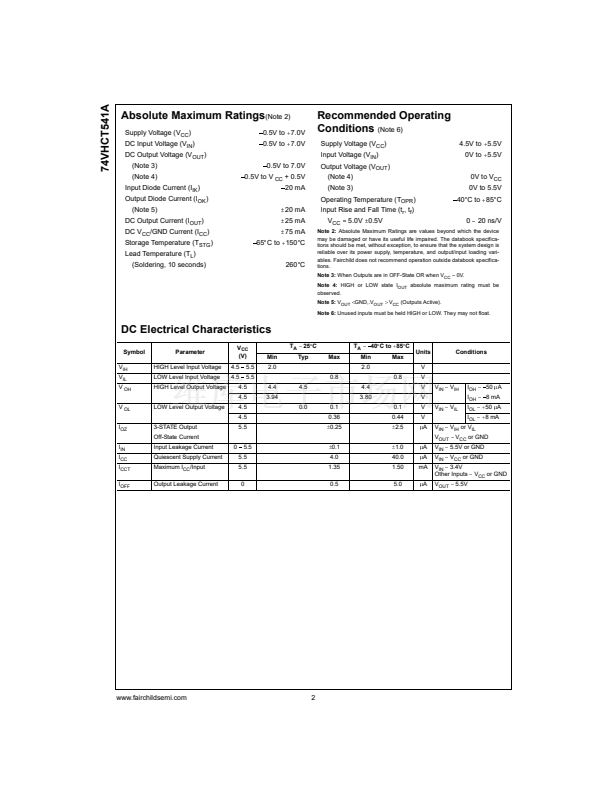
Protection circuits ensure that 0V to 7V can be applied to
the input and output (Note 1) pins without regard to the
supply voltage. This device can be used to interface 3V to
5V systems and two supply systems such as battery
backup. This circuit prevents device destruction due to mis-
matched supply and input voltages.
Note 1:
Outputs in OFF-state.
Features
s
High Speed: t
PD
5.5 ns (typ) at V
CC
5V
25
q
C
s
Low power dissipation: I
CC
4
P
A (max) at T
A
s
Power down protection is provided on all inputs and
outputs
s
Pin and function compatible with 74HCT541
Ordering Code:
Order Number
74VHCT541AM
74VHCT541ASJ
74VHCT541AMTC
74VHCT541AN
Package Number
M20B
M20D
MTC20
N20A
Package Description
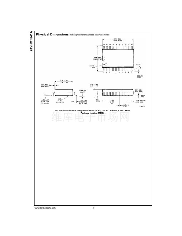
20-Lead Small Outline Integrated Circuit (SOIC), JEDEC MS-013, 0.300" Wide
Pb-Free 20-Lead Small Outline Package (SOP), EIAJ TYPE II, 5.3mm Wide
20-Lead Thin Shrink Small Outline Package (TSSOP), JEDEC MO-153, 4.4mm Wide
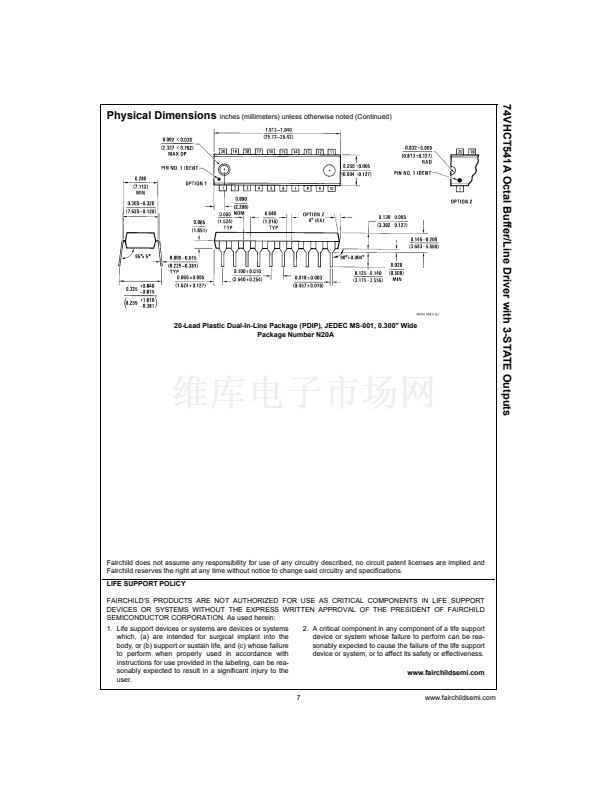
20-Lead Plastic Dual-In-Line Package (PDIP), JEDEC MS-001, 0.300" Wide
Surface mount packages are also available on Tape and Reel. Specify by appending the suffix letter 鈥淴鈥?to the ordering code.
Pb-Free package per JEDEC J-STD-020B.
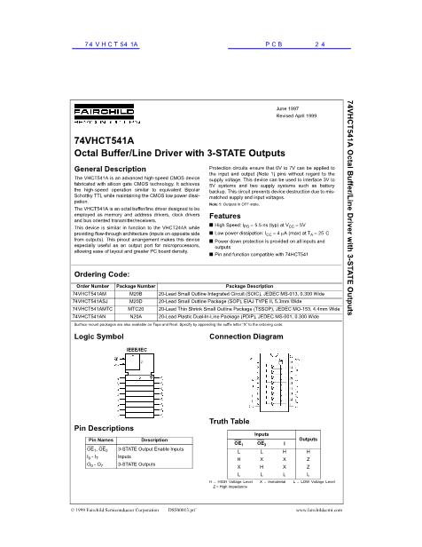
Logic Symbol
IEEE/IEC
Connection Diagram
Truth Table
Pin Descriptions
Pin Names
OE
1
, OE
2
I
0
- I
7
O
0
- O
7
Description
3-STATE Output Enable Inputs
Inputs
3-STATE Outputs
H
X
Inputs
OE
1
L
H
X
L
HIGH Voltage Level
Immaterial
Outputs
I
H
X
X
L
H
Z
Z
L
OE
2
L
X
H
L
L LOW Voltage Level
Z High Impedance
漏 2005 Fairchild Semiconductor Corporation
DS500013
www.fairchildsemi.com


 1
1
 2
2
 3
3
 4
4
 5
5
 6
6
 7
7
