80960JA/JF/JD/JT 3.3 V EMBEDDED
32-BIT MICROPROCESSOR
Advance Information Datasheet
Product Features
s
s
s
s
s
Pin/Code Compatible with all 80960Jx
Processors
High-Performance Embedded Architecture
鈥擮ne Instruction/Clock Execution
鈥擟ore Clock Rate is:
80960JA/JF 1x the Bus Clock
80960JD 2x the Bus Clock
80960JT 3x the Bus Clock
鈥擫oad/Store Programming Model
鈥擲ixteen 32-Bit Global Registers
鈥擲ixteen 32-Bit Local Registers (8 sets)
鈥擭ine Addressing Modes
鈥擴ser/Supervisor Protection Model
Two-Way Set Associative Instruction
Cache
鈥?0960JA - 2 Kbyte
鈥?0960JF/JD - 4 Kbyte
鈥?0960JT - 16 Kbyte
鈥擯rogrammable Cache-Locking
Mechanism
Direct Mapped Data Cache
鈥?0960JA - 1 Kbyte
鈥?0960JF/JD - 2 Kbyte
鈥?0960JT - 4 Kbyte
鈥擶rite Through Operation
On-Chip Stack Frame Cache
鈥擲even Register Sets Can Be Saved
鈥擜utomatic Allocation on Call/Return
鈥?-7 Frames Reserved for High-Priority
Interrupts
s
s
s
s
s
s
s
s
On-Chip Data RAM
鈥? Kbyte Critical Variable Storage
鈥擲ingle-Cycle Access
3.3 V Supply Voltage
鈥? V Tolerant Inputs
鈥擳TL Compatible Outputs
High Bandwidth Burst Bus
鈥?2-Bit Multiplexed Address/Data
鈥擯rogrammable Memory Configuration
鈥擲electable 8-, 16-, 32-Bit Bus Widths
鈥擲upports Unaligned Accesses
鈥擝ig or Little Endian Byte Ordering
High-Speed Interrupt Controller
鈥?1 Programmable Priorities
鈥擡ight Maskable Pins plus NMI
鈥擴p to 240 Vectors in Expanded Mode
Two On-Chip Timers
鈥擨ndependent 32-Bit Counting
鈥擟lock Prescaling by 1, 2, 4 or 8
鈥攍nternal Interrupt Sources
Halt Mode for Low Power
IEEE 1149.1 (JTAG) Boundary Scan
Compatibility
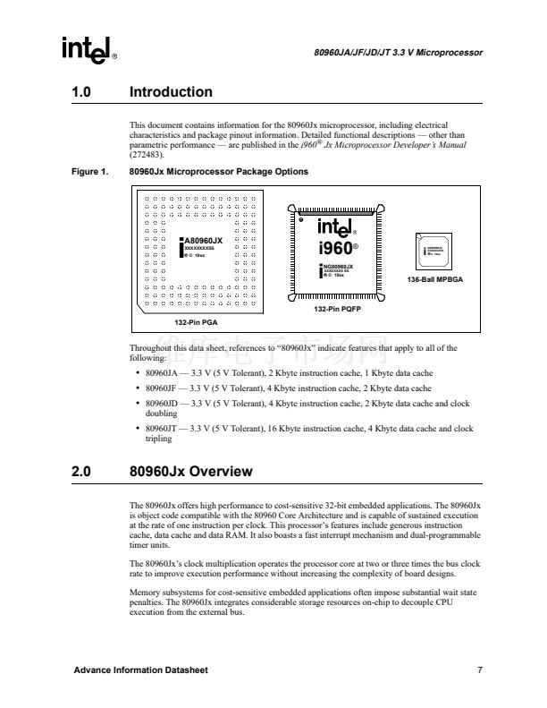
Packages
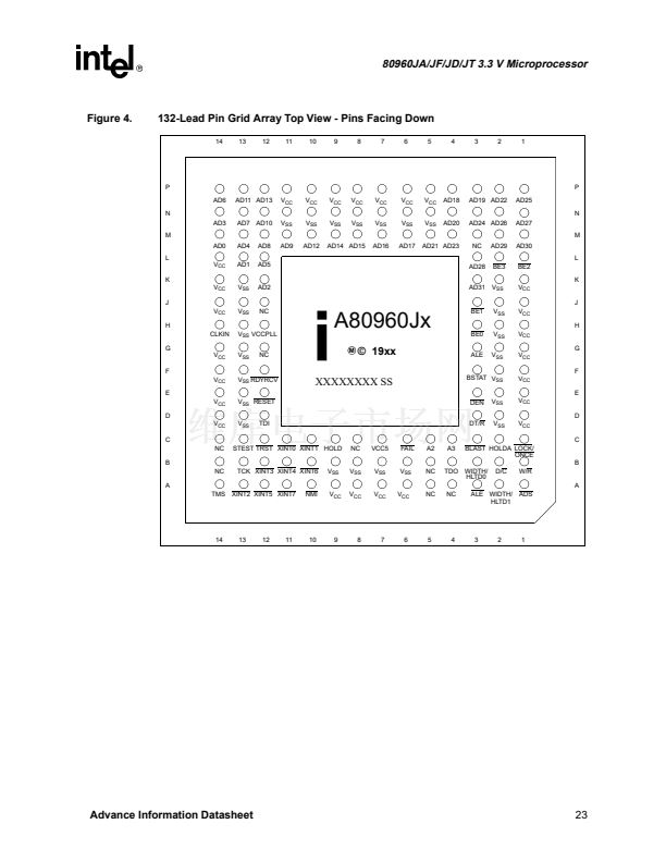
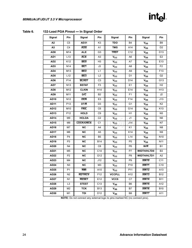
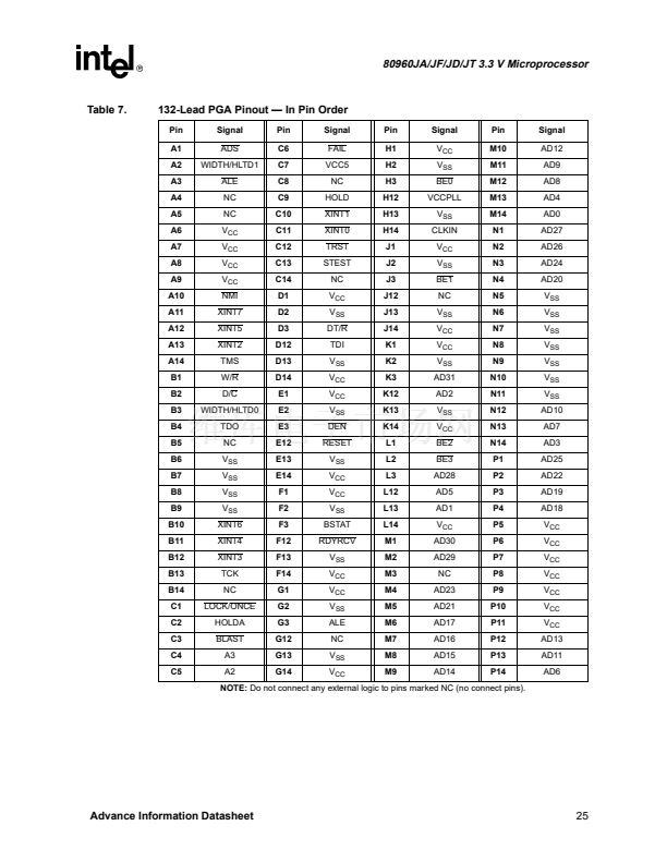
鈥?32-Lead Pin Grid Array (PGA)
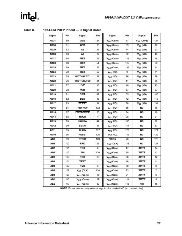
鈥?32-Lead Plastic Quad Flat Pack
(PQFP)
鈥?96-Ball Mini Plastic Ball Grid Array
(MPBGA)
Notice:
This document contains information on products in the sampling and initial production
phases of development. The specifications are subject to change without notice. Verify with your
local Intel sales office that you have the latest datasheet before finalizing a design.
Order Number: 273159-001
March, 1998


 1
1
 2
2
 3
3
 4
4
 5
5
 6
6
 7
7
 8
8
 9
9
 10
10
 11
11
 12
12
 13
13
 14
14
 15
15
 16
16
 17
17
 18
18
 19
19
 20
20
 21
21
 22
22
 23
23
 24
24
 25
25
 26
26
 27
27
 28
28
 29
29
 30
30
 31
31
 32
32
 33
33
 34
34
 35
35
 36
36
 37
37
 38
38
 39
39
 40
40
 41
41
 42
42
 43
43
 44
44
 45
45
 46
46
 47
47
 48
48
 49
49
 50
50
 51
51
 52
52
 53
53
 54
54
 55
55
 56
56
 57
57
 58
58
 59
59
 60
60
 61
61
 62
62
 63
63
 64
64
 65
65
 66
66
 67
67
 68
68
 69
69
 70
70
 71
71
 72
72
 73
73
 74
74
 75
75
 76
76
 77
77
