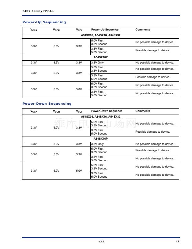
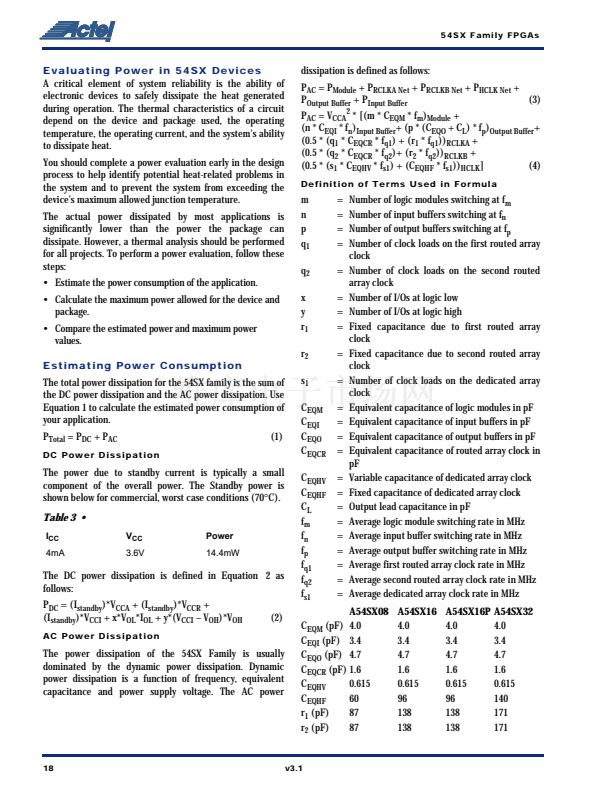
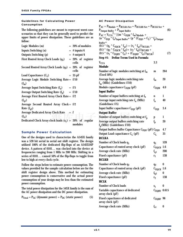
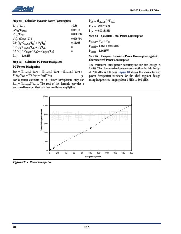
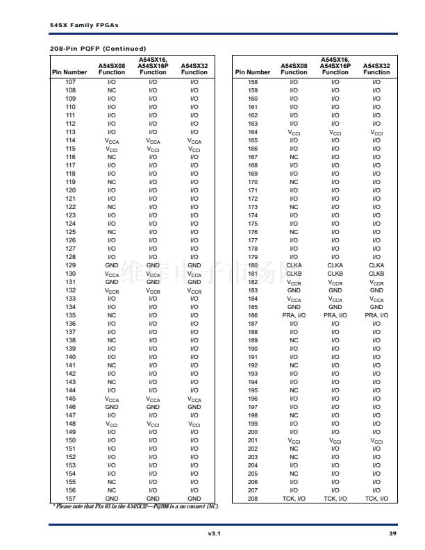
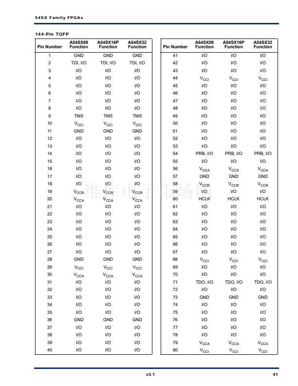
v3.1
54SX Family FPGAs
Le a di ng E dg e P er f or m a nc e
F ea t u r es
鈥?320 MHz Internal Performance
鈥?3.7 ns Clock-to-Out (Pin-to-Pin)
鈥?0.1 ns Input Set-Up
鈥?0.25 ns Clock Skew
Sp e ci f ic at ion s
鈥?66 MHz PCI
鈥?CPLD and FPGA Integration
鈥?Single Chip Solution
鈥?100% Resource Utilization with 100% Pin Locking
鈥?3.3V Operation with 5.0V Input Tolerance
鈥?Very Low Power Consumption
鈥?Deterministic, User-Controllable Timing
鈥?Unique In-System Diagnostic and Debug capability with
Silicon Explorer II
鈥?Boundary Scan Testing in Compliance with IEEE Standard
1149.1 (JTAG)
鈥?Secure Programming Technology Prevents Reverse
Engineering and Design Theft
鈥?12,000 to 48,000 System Gates
鈥?Up to 249 User-Programmable I/O Pins
鈥?Up to 1080 Flip-Flops
鈥?0.35碌 CMOS
S X P r od u c t P ro fi l e
A54SX08
Capacity
Typical Gates
System Gates
Logic Modules
Combinatorial Cells
Register Cells (Dedicated Flip-Flops)
Maximum User I/Os
Clocks
JTAG
PCI
Clock-to-Out
Input Set-Up (External)
Speed Grades
Temperature Grades
Packages (by pin count)
PLCC
PQFP
VQFP
TQFP
PBGA
FBGA
8,000
12,000
768
512
256
130
3
Yes
鈥?/div>
3.7 ns
0.8 ns
Std, 鈥?, 鈥?, 鈥?
C, I, M
84
208
100
144, 176
鈥?/div>
144
A54SX16
16,000
24,000
1,452
924
528
175
3
Yes
鈥?/div>
3.9 ns
0.5 ns
Std, 鈥?, 鈥?, 鈥?
C, I, M
鈥?/div>
208
100
176
鈥?/div>
鈥?/div>
A54SX16P
16,000
24,000
1,452
924
528
175
3
Yes
Yes
4.4 ns
0.5 ns
Std, 鈥?, 鈥?, 鈥?
C, I, M
鈥?/div>
208
100
144, 176
鈥?/div>
鈥?/div>
A54SX32
32,000
48,000
2,880
1800
1,080
249
3
Yes
鈥?/div>
4.6 ns
0.1 ns
Std, 鈥?, 鈥?, 鈥?
C, I, M
鈥?/div>
208
鈥?/div>
144, 176
313, 329
鈥?/div>
June 2003
1
漏 2003 Actel Corporation
A54SX08-1BG208相关型号PDF文件下载


 1
1
 2
2
 3
3
 4
4
 5
5
 6
6
 7
7
 8
8
 9
9
 10
10
 11
11
 12
12
 13
13
 14
14
 15
15
 16
16
 17
17
 18
18
 19
19
 20
20
 21
21
 22
22
 23
23
 24
24
 25
25
 26
26
 27
27
 28
28
 29
29
 30
30
 31
31
 32
32
 33
33
 34
34
 35
35
 36
36
 37
37
 38
38
 39
39
 40
40
 41
41
 42
42
 43
43
 44
44
 45
45
 46
46
 47
47
 48
48
 49
49
 50
50
 51
51
 52
52
 53
53
 54
54
 55
55
 56
56
 57
57
