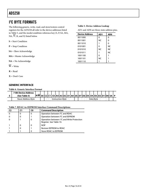
End-to-end resistance 1 k鈩? 10 k鈩? 50 k鈩? 100 k鈩?/div>
Resistance tolerance stored in EEPROM (0.1% accuracy)
Power-on EEPROM refresh time <1 ms
Software write protect command
Three-state Address Decode Pins AD0 and AD1 allow
9 packages per bus
100-year typical data retention at 55掳C
Wide operating temperature
鈭?0掳C
to +85掳C
3 V to 5 V single supply
V
DD
V
LOGIC
GND
6
I
2
C
SERIAL
INTERFACE
6
DATA
CONTROL
COMMAND
DECODE LOGIC
ADDRESS
DECODE LOGIC
CONTROL LOGIC
RDAC
EEPROM
RDAC
REGISTER
FUNCTIONAL BLOCK DIAGRAMS
RDAC
A
W
B
SCL
SDA
AD0
AD1
AD5258
05029-001
POWER-
ON RESET
Figure 1. Block Diagram
V
LOGIC
V
DD
A
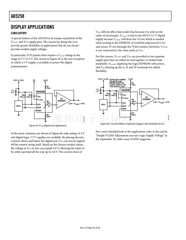
APPLICATIONS
LCD panel V
COM
adjustment
LCD panel brightness and contrast control
Mechanical potentiometer replacement in new designs
Programmable power supplies
RF amplifier biasing
Automotive electronics adjustment
Gain control and offset adjustment
Fiber to the home systems
Electronics level settings
SCL
SDA
AD0
AD1
I
2
C
SERIAL
INTERFACE
EEPROM
RDAC
REGISTER
AND
LEVEL
SHIFTER
COMMAND
DECODE LOGIC
ADDRESS
DECODE LOGIC
CONTROL
LOGIC
GND
B
W
Figure 2. Block Diagram Showing Level Shifters
GENERAL DESCRIPTION
The AD5258 provides a compact, nonvolatile 3 mm 脳 4.9 mm
packaged solution for 64-position adjustment applications.
These devices perform the same electronic adjustment function
as mechanical potentiometers
1
or variable resistors, but with
enhanced resolution and solid-state reliability.
The wiper settings are controllable through an I
2
C-compatible
digital interface that is also used to read back the wiper register
and EEPROM content. Resistor tolerance is also stored within
EEPROM providing an end-to-end tolerance accuracy of 0.1%.
There is also a software write protection function that ensures
data cannot be written to the EEPROM register.
1
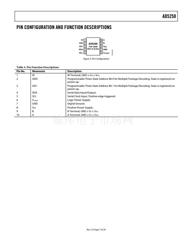
CONNECTION DIAGRAM
W
1
AD0
2
AD1
3
10
A
B
AD5258
9
SCL
5
6
V
LOGIC
Figure 3. Pinout
A separate V
LOGIC
pin delivers increased interface flexibility. For
users who need multiple parts on one bus, Address Bit AD0 and
Address Bit AD1 allow up to nine devices on the same bus.
Rev. 0
Information furnished by Analog Devices is believed to be accurate and reliable.
However, no responsibility is assumed by Analog Devices for its use, nor for any
infringements of patents or other rights of third parties that may result from its use.
Specifications subject to change without notice. No license is granted by implication
or otherwise under any patent or patent rights of Analog Devices. Trademarks and
registered trademarks are the property of their respective owners.
The terms digital potentiometer, VR (variable resistor), and RDAC are used
interchangeably.
One Technology Way, P.O. Box 9106, Norwood, MA 02062-9106, U.S.A.
Tel: 781.329.4700
www.analog.com
Fax: 781.326.8703
漏 2005 Analog Devices, Inc. All rights reserved.
05029-002
8
V
DD
TOP VIEW
(Not to Scale)
7
GND
SDA
4
05029-003


 1
1
 2
2
 3
3
 4
4
 5
5
 6
6
 7
7
 8
8
 9
9
 10
10
 11
11
 12
12
 13
13
 14
14
 15
15
 16
16
 17
17
 18
18
 19
19
 20
20
 21
21
 22
22
 23
23
 24
24
