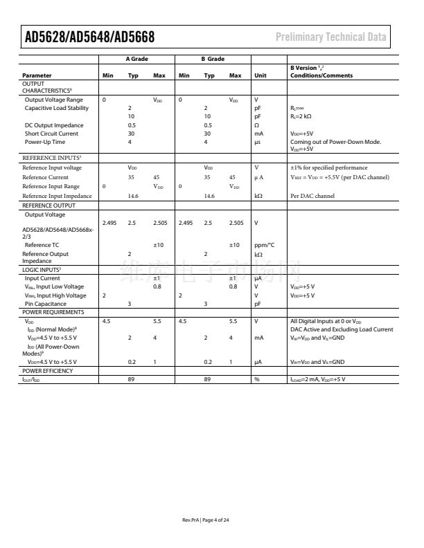
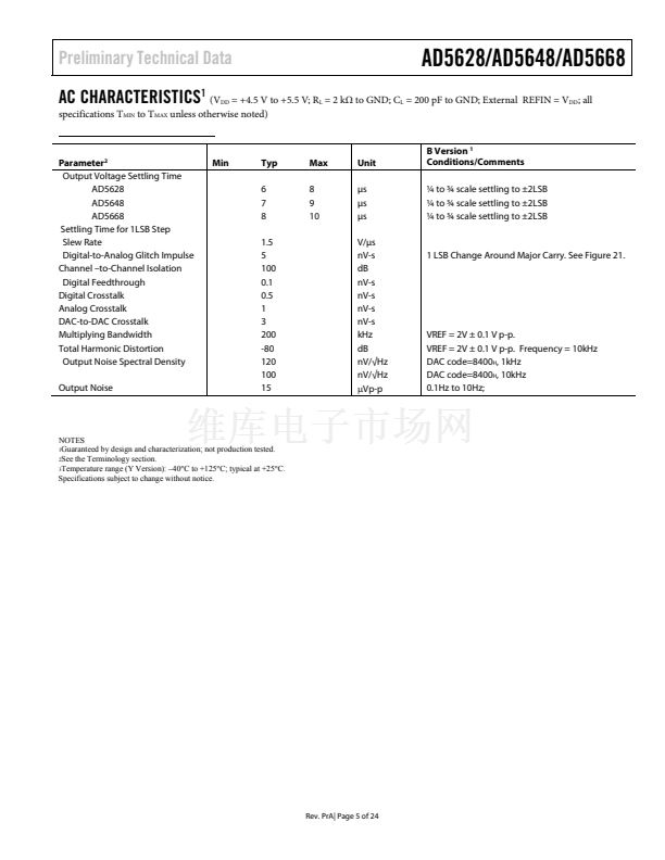
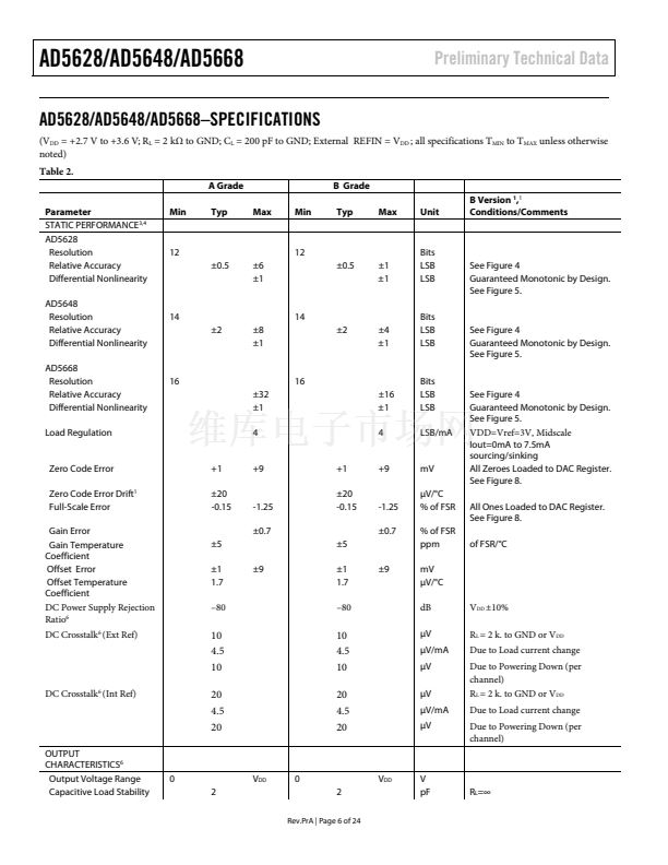
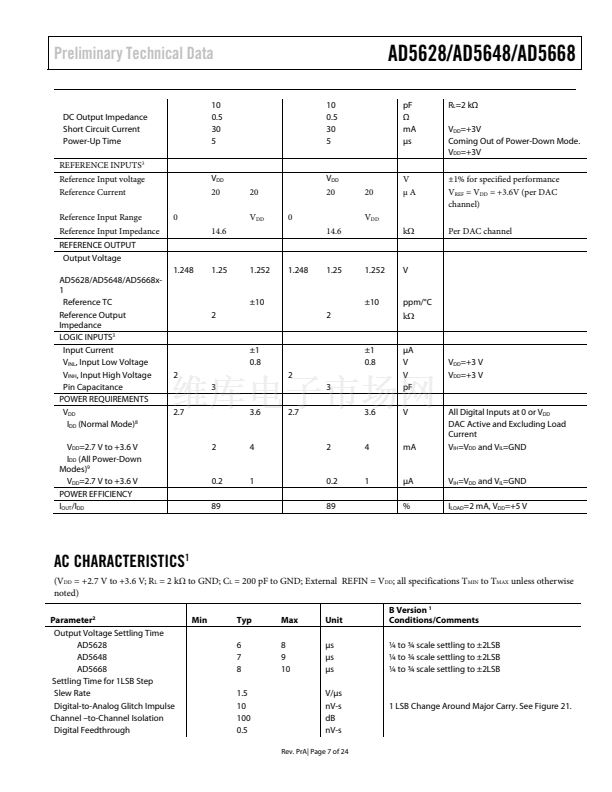
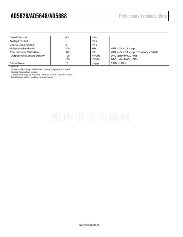
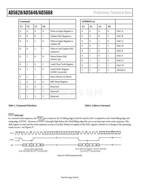
Preliminary Technical Data
FEATURES
Octal, 12-14-16 Bit Dac with 10ppm/掳C Max
On-Chip Reference in 14-Lead TSSOP
AD5628/AD5648/AD5668
Digital Gain and Offset Adjustment
Programmable Voltage and Current Sources
Programmable Attenuators
VDD
AD5628/AD5648/AD5668
I
NPUT
REGISTER
I
NPUT
REGISTER
I
NPUT
REGISTER
Low Power Smallest Pin compatible Octal DACs
AD5668: 16 Bits
AD5648: 14 Bits
AD5628: 12 Bits
12-Bit Accuracy Guaranteed
14/16-Lead TSSOP Package
On-chip 1.25/2.5V, 10ppm/掳C Reference
Power-Down to 200 nA @ 5V, 50 nA @ 3V
3V/5V Power Supply
Guaranteed Monotonic by Design
Power-On-Reset to Zero/Midscale
Three Power-Down Functions
Hardware /LDAC and /CLR functions
Rail-to-Rail Operation
Temperature Range -40掳C to +125掳C
V
REF
1.25/2.5V
Ref
DAC
REGISTER
DAC
REGISTER
DAC
REGISTER
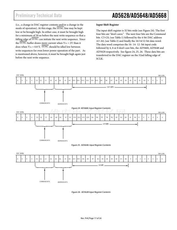
STRING
DAC A
STRING
DAC B
STRING
DAC C
STRING
DAC D
BUFFER
LDAC
VOUTA
VOUTB
VOUTC
VOUTD
VOUTE
VOUTF
VOUTG
VOUTH
BUFFER
BUFFER
SCLK
INTERFACE
LOGIC
I
NPUT
REGISTER
I
NPUT
REGIS-
TER
I
NPUT
REGISTER
I
NPUT
REGISTER
I
NPUT
REGISTER
D
AC
REGISTER
D
AC
REGISTER
D
AC
REGISTER
D
AC
REGISTER
D
AC
REGISTER
BUFFER
SYNC
STRING
DAC E
STRING
DAC F
STRING
DAC G
STRING
DAC H
BUFFER
DIN
BUFFER
BUFFER
BUFFER
POWER-ON
RESET
POWER-DOWN
LOGIC
APPLICATIONS
ProcessControl
Data Acquisition Systems
Portable Battery Powered Instruments
LDAC* CLR*
*RU-16 PACKAGE ONLY
GND
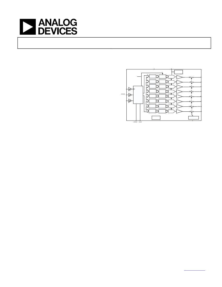
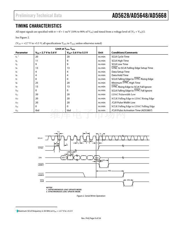
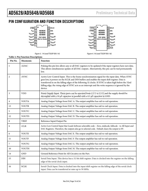
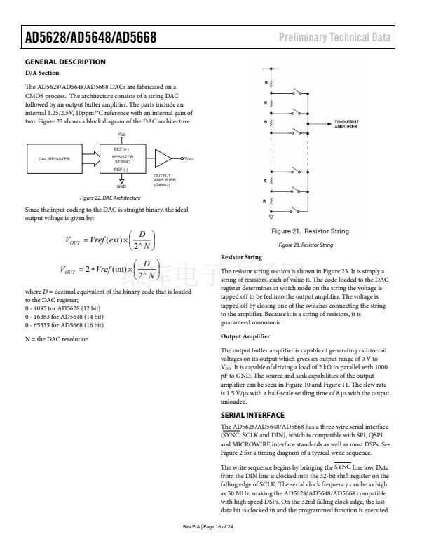
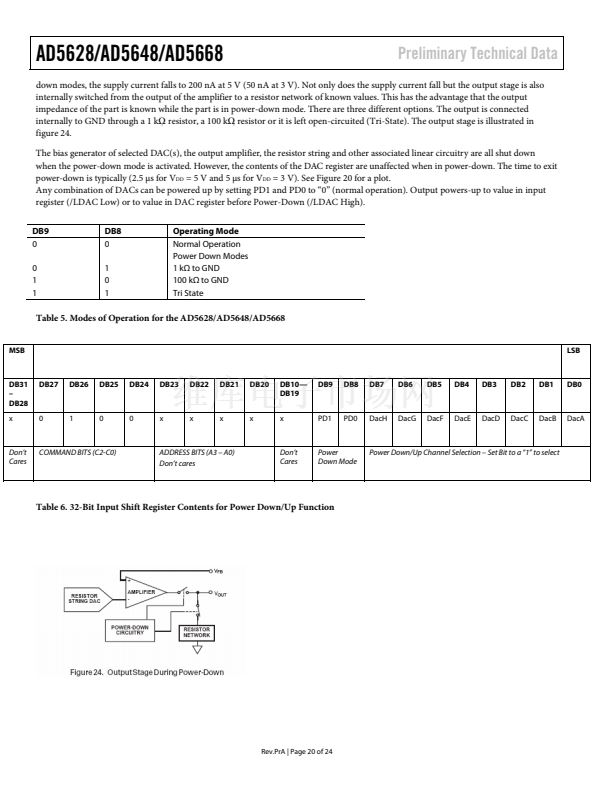
Figure 1. Functional Block Diagram
GENERAL DESCRIPTION
The AD5628/48/68 family of devices are low power, octal, 12-
14-16-bit buffered voltage-out DACs. All devices operate from
a single +2.7V to +5.5V, and are guaranteed monotonic by
design.
The AD5628/48/68 have an on-chip reference with an internal
gain of two. The AD56x8-1 has a 1.25V 10ppm/掳C max
reference and the AD56x8-2,-3 have a 2.5V 10ppm/掳C max
reference. The on-board reference is off at power-up allowing
the use of an external reference. The internal reference is
turned on by writing to the DAC. The part incorporates a
power-on-reset circuit that ensures that the DAC output
powers up to zero volts (AD56x8-1,-2/) or midscale (AD5668-
3) and remains there until a valid write takes place. The part
contains a power-down feature that reduces the current
consumption of the device to 200nA at 5V and provides
software selectable output loads while in power-down mode for
any or all DACs channels.
The outputs of all DACs may be updated simultaneously using
the /LDAC function, with the added functionality of selecting
through software any number of DAC channels to synchronize.
There is also an asynchronous active low /CLR that clears all
DACs to a software selectable code - 0 V, midscale or fullscale .
The AD5628/48/68 utilizes a versatile three-wire serial
interface that operates at clock rates up to 50 MHz and is
compatible with standard SPI鈩? QSPI鈩? MICROWIRE鈩?and
DSP interface standards. Its on-chip precision output amplifier
allows rail-to-rail output swing to be achieved.
PRODUCT HIGHLIGHTS
1.
2.
3.
4.
5.
Octal 12/14/16-Bit DAC; 12-Bit Accuracy Guaranteed.
On-chip 1.25/2.5V, 10ppm/掳C max Reference.
Available in 14/16-lead TSSOP package.
Power-On-Reset to Zero volts or Midscale.
Power-down capability. When powered down, the
DAC typically consumes 50nA at 3V and 200nA at 5V.
Rev. PrA
Information furnished by Analog Devices is believed to be accurate and reliable.
However, no responsibility is assumed by Analog Devices for its use, nor for any
infringements of patents or other rights of third parties that may result from its use.
Specifications subject to change without notice. No license is granted by implication
or otherwise under any patent or patent rights of Analog Devices. Trademarks and
registered trademarks are the property of their respective companies.
One Technology Way, P.O. Box 9106, Norwood, MA 02062-9106, U.S.A.
www.analog.com
Tel: 781.329.4700
Fax: 781.326.8703
漏 2004 Analog Devices, Inc. All rights reserved.


 1
1
 2
2
 3
3
 4
4
 5
5
 6
6
 7
7
 8
8
 9
9
 10
10
 11
11
 12
12
 13
13
 14
14
 15
15
 16
16
 17
17
 18
18
 19
19
 20
20
 21
21
 22
22
 23
23
 24
24
