鈩?/div>
process technology
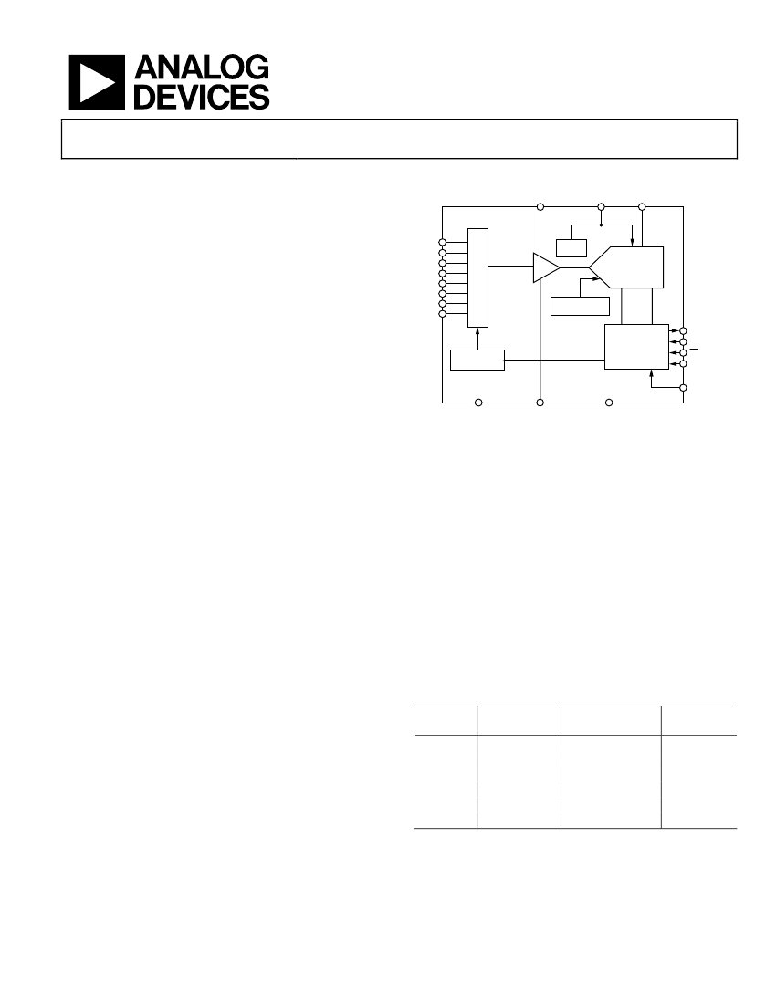
FUNCTIONAL BLOCK DIAGRAM
V
DD
REFIN/OUT
V
CC
AD7328
V
IN
0
V
IN
1
V
IN
2
V
IN
3
V
IN
4
V
IN
5
V
IN
6
V
IN
7
I/P
MUX
T/H
2.5V
VREF
13-BIT
SUCCESSIVE
APPROXIMATION
ADC
TEMPERATURE
INDICATOR
DOUT
CONTROL LOGIC
AND REGISTERS
SCLK
CS
DIN
V
DRIVE
AGND
V
SS
DGND
CHANNEL
SEQUENCER
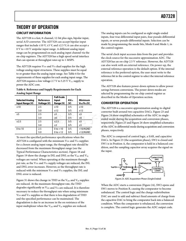
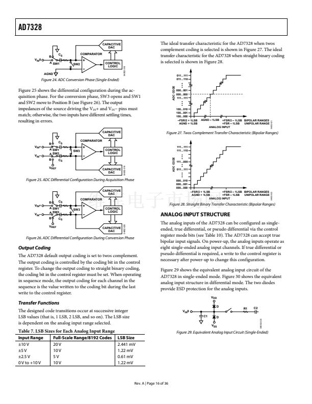
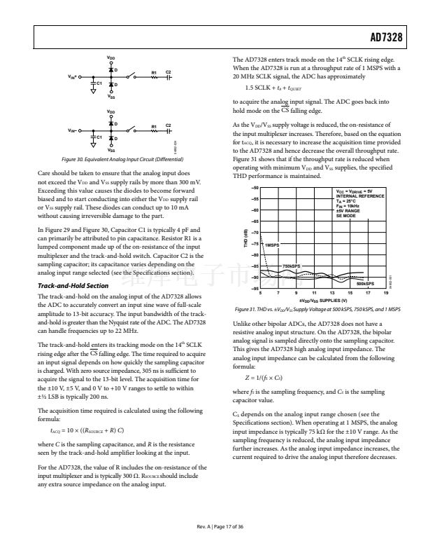
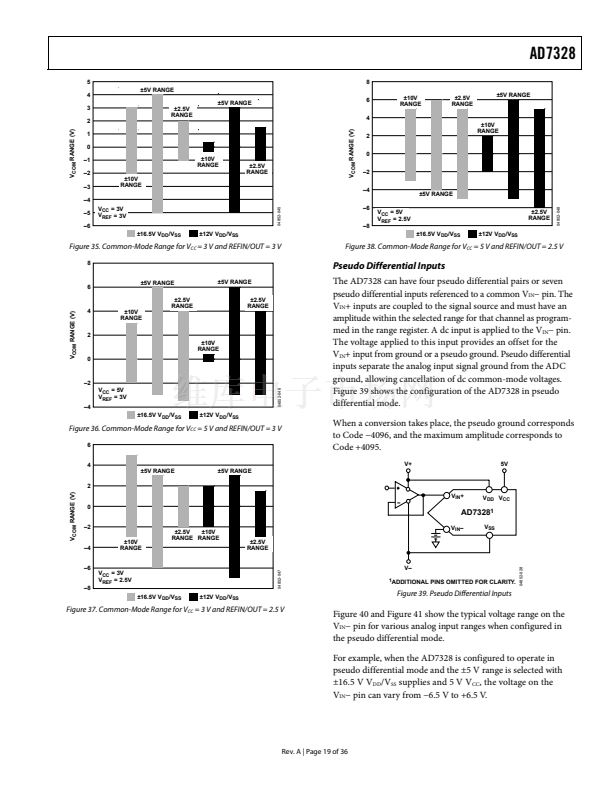
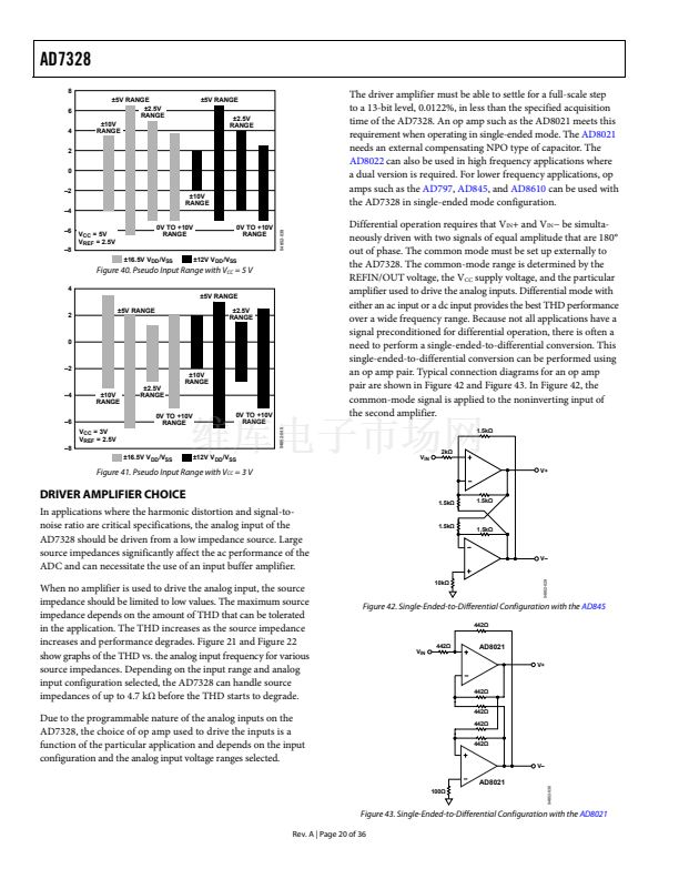
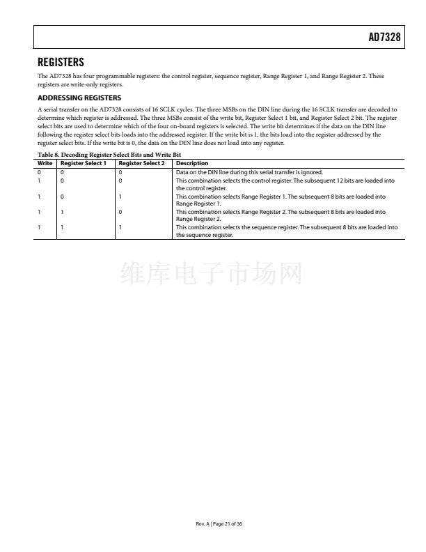
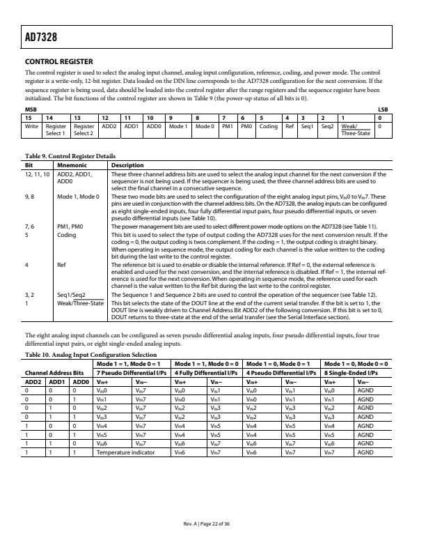
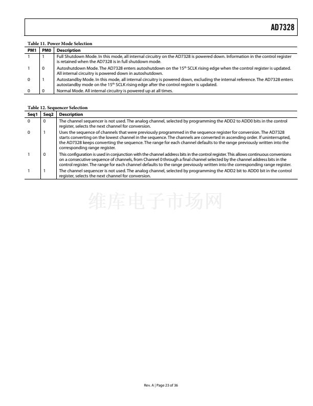
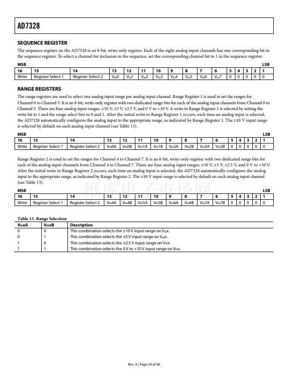
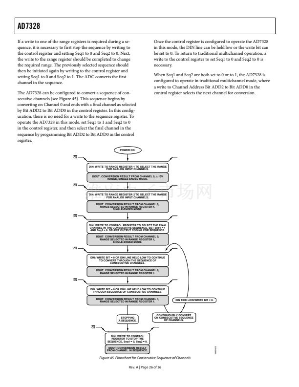
Figure 1.
GENERAL DESCRIPTION
The AD7328
1
is an 8-channel, 12-bit plus sign, successive
approximation ADC designed on the
iCMOS
(industrial
CMOS) process.
iCMOS
is a process combining high voltage
silicon with submicron CMOS and complementary bipolar
technologies. It enables the development of a wide range of high
performance analog ICs capable of 33 V operation in a footprint
that no previous generation of high voltage parts could achieve.
Unlike analog ICs using conventional CMOS processes,
iCMOS
components can accept bipolar input signals while providing
increased performance, dramatically reduced power consumption,
and reduced package size.
The AD7328 can accept true bipolar analog input signals. The
AD7328 has four software-selectable input ranges, 卤10 V, 卤5 V,
卤2.5 V, and 0 V to +10 V. Each analog input channel can be
independently programmed to one of the four input ranges. The
analog input channels on the AD7328 can be programmed to be
single-ended, true differential, or pseudo differential.
The ADC contains a 2.5 V internal reference. The AD7328 also
allows for external reference operation. If a 3 V reference is applied
to the REFIN/OUT pin, the AD7328 can accept a true bipolar
卤12 V analog input. Minimum 卤12 V V
DD
and V
SS
supplies are
required for the 卤12 V input range. The ADC has a high speed
serial interface that can operate at throughput rates up to 1 MSPS.
PRODUCT HIGHLIGHTS
1.
2.
The AD7328 can accept true bipolar analog input signals,
卤10 V, 卤5 V, 卤2.5 V, and 0 V to +10 V unipolar signals.
The eight analog inputs can be configured as eight single-
ended inputs, four true differential input pairs, four pseudo
differential inputs, or seven pseudo differential inputs.
1 MSPS serial interface. SPI庐-/QSPI鈩?/DSP-/MICROWIRE鈩?
compatible interface.
Low power, 30 mW, at a maximum throughput rate of
1 MSPS.
Channel sequencer.
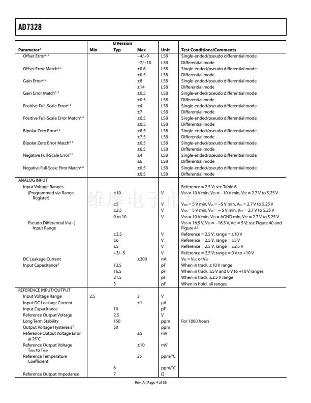
Throughput
Rate
1000 kSPS
500 kSPS
1000 kSPS
500 kSPS
1000 kSPS
500 kSPS
Number of
Channels
8
8
4
4
2
2
3.
4.
5.
Table 1. Similar Product Selection
Device
Number
AD7329
AD7327
AD7324
AD7323
AD7322
AD7321
Number of Bits
12-bit plus sign
12-bit plus sign
12-bit plus sign
12-bit plus sign
12-bit plus sign
12-bit plus sign
1
Protected by U.S. Patent No. 6,731,232.
Rev. A
Information furnished by Analog Devices is believed to be accurate and reliable. However, no
responsibility is assumed by Analog Devices for its use, nor for any infringements of patents or other
rights of third parties that may result from its use. Specifications subject to change without notice. No
license is granted by implication or otherwise under any patent or patent rights of Analog Devices.
Trademarks and registered trademarks are the property of their respective owners.
One Technology Way, P.O. Box 9106, Norwood, MA 02062-9106, U.S.A.
Tel: 781.329.4700
www.analog.com
Fax: 781.461.3113
漏2006 Analog Devices, Inc. All rights reserved.
04852-001


 1
1
 2
2
 3
3
 4
4
 5
5
 6
6
 7
7
 8
8
 9
9
 10
10
 11
11
 12
12
 13
13
 14
14
 15
15
 16
16
 17
17
 18
18
 19
19
 20
20
 21
21
 22
22
 23
23
 24
24
 25
25
 26
26
 27
27
 28
28
 29
29
 30
30
 31
31
 32
32
 33
33
 34
34
 35
35
 36
36
