a
1 pC Charge Injection, 100 pA Leakage,
CMOS 5 V/+5 V/+3 V Quad SPST Switches
ADG611/ADG612/ADG613
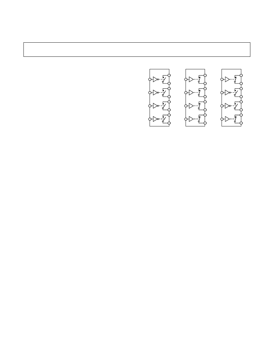
FUNCTIONAL BLOCK DIAGRAMS
ADG611
S1
IN1
D1
S2
IN2
D2
S3
IN3
D3
S4
IN4
IN4
D4
D4
IN3
D3
S4
IN4
D4
IN2
D2
S3
IN3
D3
S4
IN1
D1
S2
IN2
D2
S3
FEATURES
1 pC Charge Injection
2.7 V to 5.5 V Dual Supply
+2.7 V to +5.5 V Single Supply
Automotive Temperature Range 鈥?0 C to +125 C
100 pA Max @ 25 C Leakage Currents
85 On-Resistance
Rail-to-Rail Switching Operation
Fast Switching Times
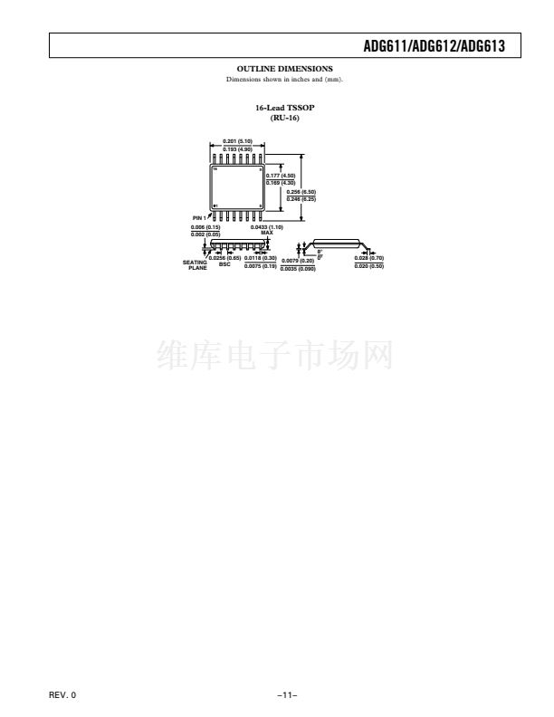
16-Lead TSSOP Packages
Typical Power Consumption (<0.1 W)
TTL/CMOS-Compatible Inputs
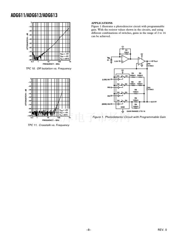
APPLICATIONS
Automatic Test Equipment
Data Acquisition Systems
Battery-Powered Systems
Communication Systems
Sample and Hold Systems
Audio Signal Routing
Relay Replacement
Avionics
ADG612
S1
IN1
ADG613
S1
D1
S2
SWITCHES SHOWN FOR A LOGIC 鈥?鈥?INPUT
GENERAL DESCRIPTION
PRODUCT HIGHLIGHTS
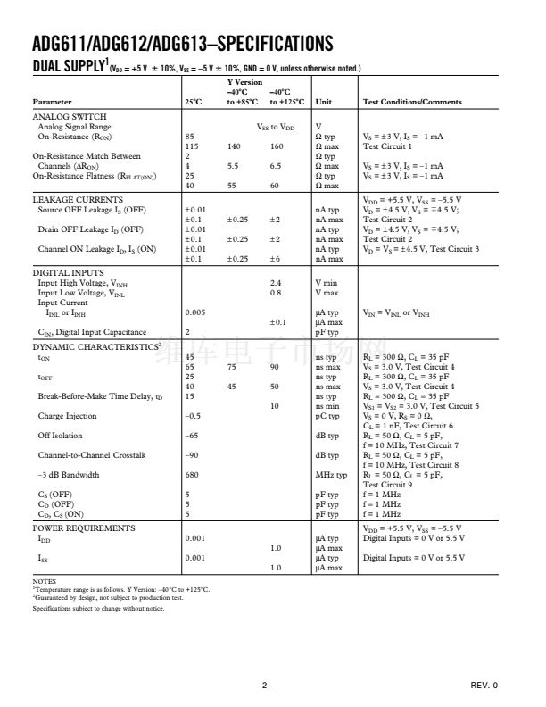
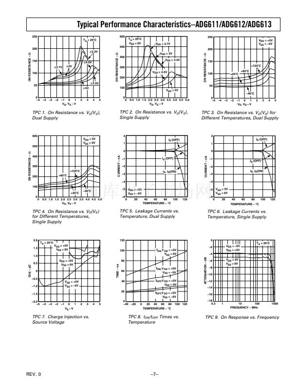
The ADG611, ADG612, and ADG613 are monolithic CMOS
devices containing four independently selectable switches. These
switches offer ultralow charge injection of 1 pC over full input
signal range and typical leakage currents of 10 pA at 25掳C.
They are fully specified for
卤
5 V, +5 V, and +3 V supplies.
They contain four independent single-pole/single-throw (SPST)
switches. The ADG611 and ADG612 differ only in that the
digital control logic is inverted. The ADG611 switches are turned
on with a logic low on the appropriate control input, while a logic
high is required to turn on the switches of the ADG612. The
ADG613 contains two switches whose digital control logic is
similar to the ADG611, while the logic is inverted on the other
two switches.
Each switch conducts equally well in both directions when ON
and has an input signal range that extends to the supplies. The
ADG613 exhibits break-before-make switching action. The
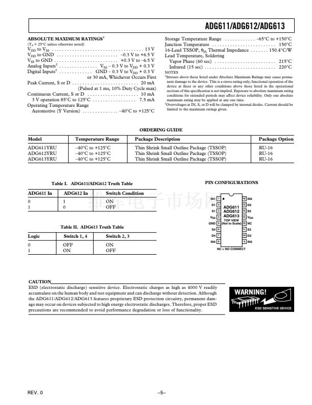
ADG611/ADG612/ADG613 are available in small 16-lead
TSSOP packages.
1. Ultralow Charge Injection (1 pC typically)
2. Dual
卤
2.7 V to
卤
5.5 V or Single +2.7 V to +5.5 V
Operation.
3. Automotive Temperature Range, 鈥?0掳C to +125掳C
4. Small 16-lead TSSOP package.
REV. 0
Information furnished by Analog Devices is believed to be accurate and
reliable. However, no responsibility is assumed by Analog Devices for its
use, nor for any infringements of patents or other rights of third parties that
may result from its use. No license is granted by implication or otherwise
under any patent or patent rights of Analog Devices.
One Technology Way, P.O. Box 9106, Norwood, MA 02062-9106, U.S.A.
Tel: 781/329-4700
www.analog.com
Fax: 781/326-8703
漏 Analog Devices, Inc., 2002


 1
1
 2
2
 3
3
 4
4
 5
5
 6
6
 7
7
 8
8
 9
9
 10
10
 11
11
 12
12
