鈥?/div>
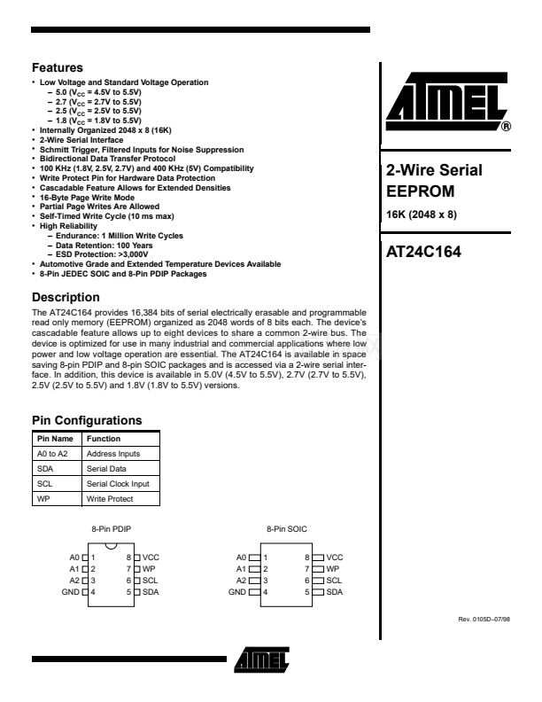
Low Voltage and Standard Voltage Operation
鈥?5.0 (V
CC
= 4.5V to 5.5V)
鈥?2.7 (V
CC
= 2.7V to 5.5V)
鈥?2.5 (V
CC
= 2.5V to 5.5V)
鈥?1.8 (V
CC
= 1.8V to 5.5V)
Internally Organized 2048 x 8 (16K)
2-Wire Serial Interface
Schmitt Trigger, Filtered Inputs for Noise Suppression
Bidirectional Data Transfer Protocol
100 KHz (1.8V, 2.5V, 2.7V) and 400 KHz (5V) Compatibility
Write Protect Pin for Hardware Data Protection
Cascadable Feature Allows for Extended Densities
16-Byte Page Write Mode
Partial Page Writes Are Allowed
Self-Timed Write Cycle (10 ms max)
High Reliability
鈥?Endurance: 1 Million Write Cycles
鈥?Data Retention: 100 Years
鈥?ESD Protection: >3,000V
Automotive Grade and Extended Temperature Devices Available
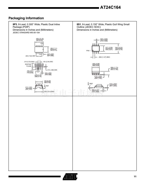
8-Pin JEDEC SOIC and 8-Pin PDIP Packages
鈥?/div>
鈥?/div>
鈥?/div>
鈥?/div>
鈥?/div>
鈥?/div>
鈥?/div>
鈥?/div>
鈥?/div>
鈥?/div>
鈥?/div>
2-Wire Serial
EEPROM
16K (2048 x 8)
AT24C164
鈥?/div>
鈥?/div>
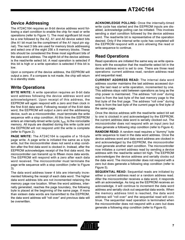
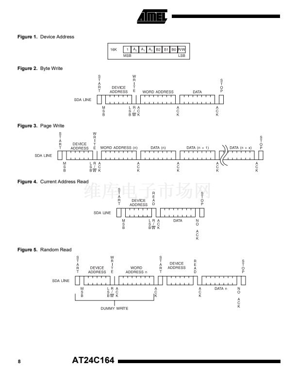
Description
The AT24C164 provides 16,384 bits of serial electrically erasable and programmable
read only memory (EEPROM) organized as 2048 words of 8 bits each. The device鈥檚
cascadable feature allows up to eight devices to share a common 2-wire bus. The
device is optimized for use in many industrial and commercial applications where low
power and low voltage operation are essential. The AT24C164 is available in space
saving 8-pin PDIP and 8-pin SOIC packages and is accessed via a 2-wire serial inter-
face. In addition, this device is available in 5.0V (4.5V to 5.5V), 2.7V (2.7V to 5.5V),
2.5V (2.5V to 5.5V) and 1.8V (1.8V to 5.5V) versions.
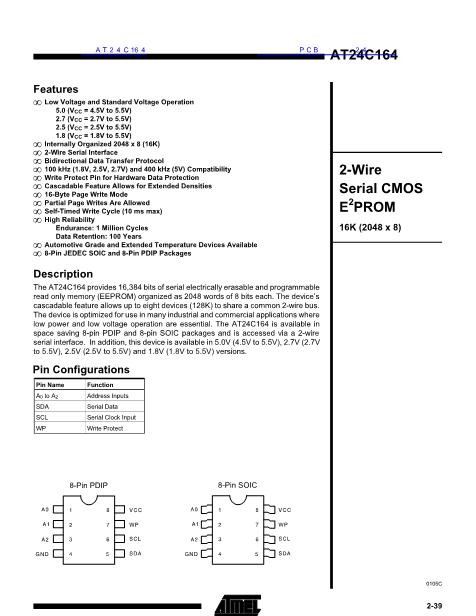
Pin Configurations
Pin Name
A0 to A2
SDA
SCL
WP
Function
Address Inputs
Serial Data
Serial Clock Input
Write Protect
2-Wire, 16K
Serial EEPROM
8-Pin PDIP
8-Pin SOIC
A0
A1
A2
GND
1
2
3
4
8
7
6
5
VCC
WP
SCL
SDA
A0
A1
A2
GND
1
2
3
4
8
7
6
5
VCC
WP
SCL
SDA
Rev. 0105D鈥?7/98
1


 1
1
 2
2
 3
3
 4
4
 5
5
 6
6
 7
7
 8
8
 9
9
 10
10
 11
11
