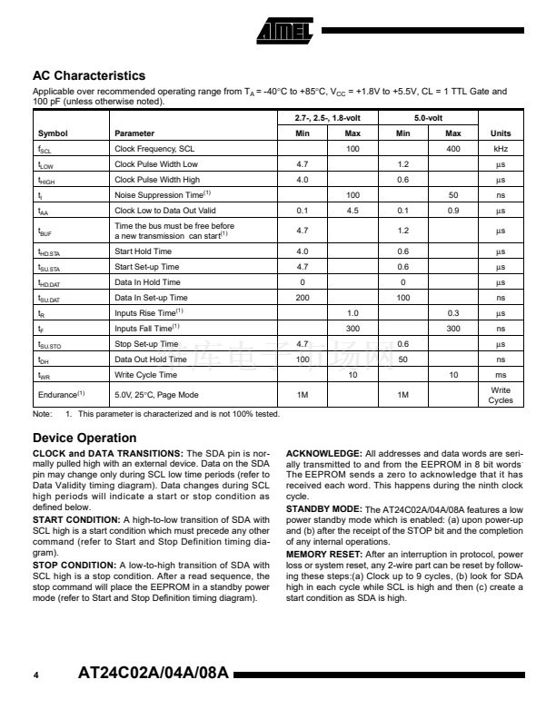
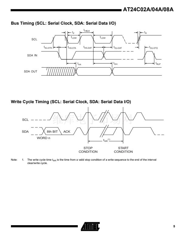
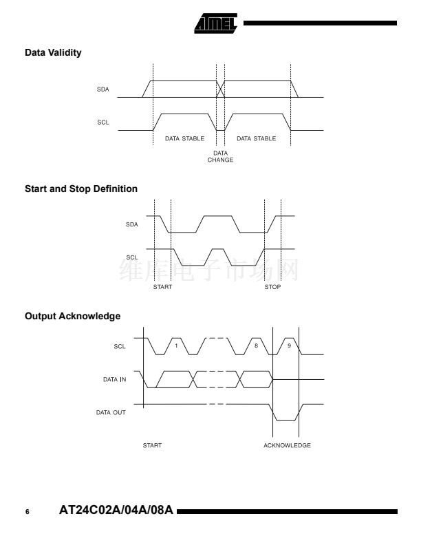
鈥?/div>
鈥?Utilizes Different Array Protection Compared to the AT24C02/04/08
Low Voltage and Standard Voltage Operation
鈥?5.0 (V
CC
= 4.5V to 5.5V)
鈥?2.7 (V
CC
= 2.7V to 5.5V)
鈥?2.5 (V
CC
= 2.5V to 5.5V)
鈥?1.8 (V
CC
= 1.8V to 5.5V)
Internally Organized 256 x 8 (2K), 512 x 8 (4K) or 1024 x 8 (8K)
2-Wire Serial Interface
Schmitt Trigger, Filtered Inputs for Noise Supperssion
Bidirectional Data Transfer Protocol
100 kHz (1.8V, 2.5V, 2.7V) and 400 kHz (5V) Compatibility
8-Byte Page (2K), 16-Byte Page (4K, 8K) Write Modes
Partial Page Writes Are Allowed
Self-Timed Write Cycle (10 ms max)
High Reliability
鈥?Endurance: 1 Million Write Cycles
鈥?Data Retention: 100 Years
鈥?ESD Protection: >3000V
Automotive Grade and Extended Temperature Devices Available
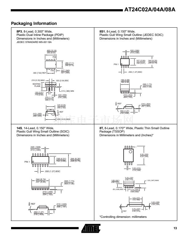
8-Pin and 14-Pin JEDEC SOIC, 8-Pin PDIP, and 8-Pin TSSOP Packages
鈥?/div>
鈥?/div>
鈥?/div>
鈥?/div>
鈥?/div>
鈥?/div>
鈥?/div>
鈥?/div>
鈥?/div>
2-Wire Serial
EEPROM
2K (256 x 8)
4K (512 x 8)
8K (1024 x 8)
鈥?/div>
鈥?/div>
Description
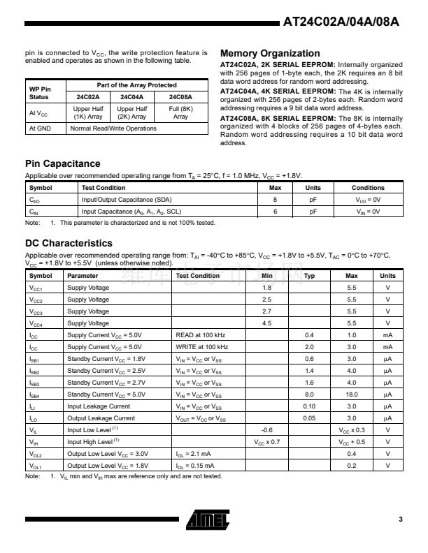
The AT24C02A/04A/08A provides 2048/4096/8192 bits of serial electrically erasable
and programmable read only memory (EEPROM) organized as 256/512/1024 words
of 8 bits each. The device is optimized for use in many industrial and commercial
applications where low power and low voltage operation are essential. The
AT24C02A/04A/08A is available in space saving 8-pin PDIP, 8-pin, 14-pin SOIC, and
8-pin TSSOP packages and is accessed via a 2-wire serial interface. In addition, the
entire family is available in 5.0V (4.5V to 5.5V), 2.7V (2.7V to 5.5V), 2.5V (2.5V to
5.5V) and 1.8V (1.8V to 5.5V) versions.
AT24C02A
AT24C04A
AT24C08A
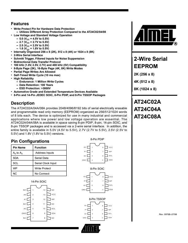
Pin Configurations
Pin Name
A
0
to A
2
SDA
SCL
WP
NC
Function
Address Inputs
Serial Data
Serial Clock Input
Write Protect
No Connect
14-Pin SOIC
8-Pin PDIP
AT24C02A/04A/
08A
8-Pin SOIC
8-Pin TSSOP
Rev. 0976B鈥?7/98
1


 1
1
 2
2
 3
3
 4
4
 5
5
 6
6
 7
7
 8
8
 9
9
 10
10
 11
11
 12
12
 13
13
