BSI
FEATURES
Very Low Power/Voltage CMOS SRAM
64K X 16 bit
DESCRIPTION
BS616LV1013
鈥?Very low operation voltage : 2.7 ~ 3.6V
鈥?Very low power consumption :
Vcc = 3.0V
C-grade : 20mA (Max.) operating current
I - grade : 25mA (Max.) operating current
0.02uA (Typ.) CMOS standby current
High speed access time :
-70
70ns (Max.) at Vcc = 3.0V
鈥?Automatic power down when chip is deselected
鈥?Three state outputs and TTL compatible
鈥?Fully static operation
鈥?Data retention supply voltage as low as 1.5V
鈥?Easy expansion with CE and OE options
鈥?I/O Configuration x8/x16 selectable by LB and UB pin
The BS616LV1013 is a high performance, very low power CMOS Static
Random Access Memory organized as 65,536 words by 16 bits and
operates from a wide range of 2.7V to 3.6V supply voltage.
Advanced CMOS technology and circuit techniques provide both high
speed and low power features with a typical CMOS standby current
of 0.02uA and maximum access time of 70ns in 3.0V operation.
Easy memory expansion is provided by an active LOW chip
enable(CE) and active LOW output enable(OE) and three-state output
drivers.
The BS616LV1013 has an automatic power down feature, reducing the
power consumption significantly when chip is deselected.
The BS616LV1013 is available in the JEDEC standard 44-pin TSOP
Type II and 48-pin BGA package.
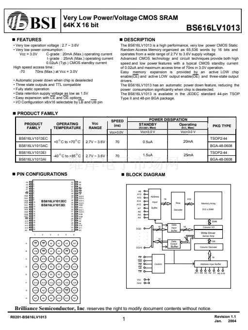
PRODUCT FAMILY
PRODUCT
FAMILY
BS616LV1013EC
BS616LV1013AC
BS616LV1013EI
BS616LV1013AI
OPERATING
TEMPERATURE
Vcc
RANGE
SPEED
(ns)
Vcc=3.0V
POWER DISSIPATION
STANDBY
Operating
(I
CCSB1
, Max)
(I
CC
, Max)
PKG TYPE
TSOP2-44
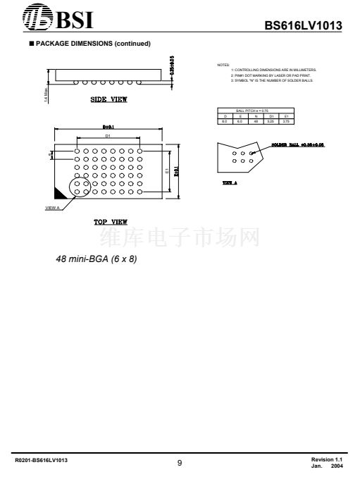
BGA-48-0608
Vcc=3.0 V
Vcc=3.0 V
+0 C to +70 C
O
O
O
O
2.7V ~ 3.6V
70
0.5uA
20mA
-40 C to +85 C
2.7V ~ 3.6V
70
1.5uA
25mA
TSOP2-44
BGA-48-0608
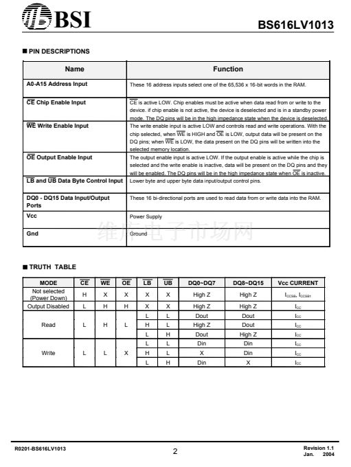
PIN CONFIGURATIONS
A4
A3
A2
A1
A0
CE
DQ0
DQ1
DQ2
DQ3
VCC
GND
DQ4
DQ5
DQ6
DQ7
WE
A15
A14
A13
A12
NC
1
2
3
4
5
6
7
8
9
10
11
12
13
14
15
16
17
18
19
20
21
22
1
44
43
42
41
40
39
38
37
36
35
34
33
32
31
30
29
28
27
26
25
24
23
6
A5
A6
A7
OE
UB
LB
DQ15
DQ14
DQ13
DQ12
GND
VCC
DQ11
DQ10
DQ9
DQ8
NC
A8
A9
A10
A11
NC
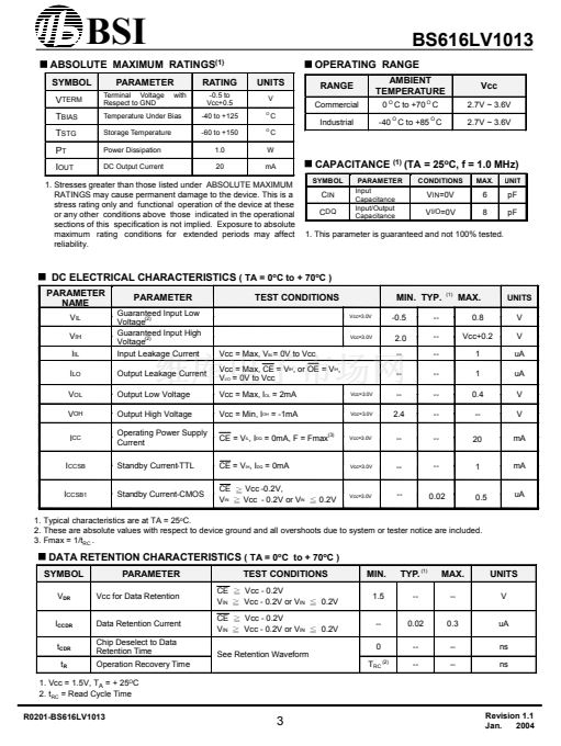
BLOCK DIAGRAM
A8
A13
A15
A14
A12
A7
A6
A5
A4
Address
Input
Buffer
BS616LV1013EC
BS616LV1013EI
18
Row
Decoder
512
Memory Array
512 x 2048
2048
DQ0
16
Data
Input
Buffer
16
Column I/O
2
3
4
5
A
LB
OE
A0
A1
A2
NC
.
.
.
.
DQ15
.
.
.
.
Write Driver
Sense Amp
128
Column Decoder
16
Data
Output
16
Buffer
B
IO8
UB
A3
A4
CE
IO0
C
IO9
IO10
A5
A6
IO1
IO2
CE
WE
OE
UB
LB
Control
14
Address Input Buffer
D
VSS
IO11
NC
A7
IO3
VCC
E
VCC
IO12
NC
NC
IO4
VSS
A11 A9 A3 A2 A1 A0 A10
F
IO14
IO13
A14
A15
IO5
IO6
Vcc
Gnd
G
IO15
NC
A12
A13
WE
IO7
H
NC
A8
A9
A10
A11
NC
Brilliance Semiconductor, Inc
.
reserves the right to modify document contents without notice.
R0201-BS616LV1013
1
Revision 1.1
Jan.
2004


 1
1
 2
2
 3
3
 4
4
 5
5
 6
6
 7
7
 8
8
 9
9
