Philips Semiconductors
Product specification
Thyristors
logic level
GENERAL DESCRIPTION
Glass passivated, sensitive gate
thyristors in a plastic envelope
suitable for surface mounting,
intended for use in general purpose
switching
and
phase
control
applications. These devices are
intended to be interfaced directly to
microcontrollers, logic integrated
circuits and other low power gate
trigger circuits.
BT148W series
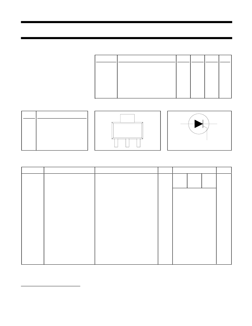
QUICK REFERENCE DATA
SYMBOL
V
DRM
,
V
RRM
I
T(AV)
I
T(RMS)
I
TSM
PARAMETER
BT148W-
Repetitive peak off-state
voltages
Average on-state current
RMS on-state current
Non-repetitive peak on-state
current
MAX. MAX. MAX. UNIT
400R
400
0.6
1
10
500R
500
0.6
1
10
600R
600
0.6
1
10
V
A
A
A
PINNING - SOT223
PIN
1
2
3
tab
DESCRIPTION
cathode
anode
gate
anode
PIN CONFIGURATION
4
SYMBOL
a
k
1
2
3
g
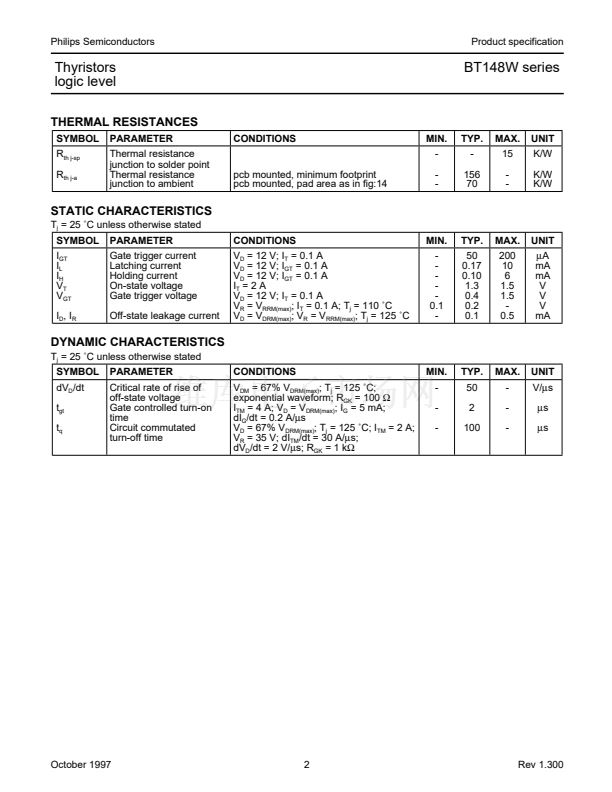
LIMITING VALUES
Limiting values in accordance with the Absolute Maximum System (IEC 134).
SYMBOL
PARAMETER
CONDITIONS
MIN.
-
half sine wave; T
sp
鈮?/div>
112 藲C
all conduction angles
half sine wave; T
j
= 25 藲C prior to
surge
t = 10 ms
t = 8.3 ms
t = 10 ms
I
TM
= 4 A; I
G
= 200 mA;
dI
G
/dt = 200 mA/碌s
-
-
-
-
-
-
-
-
-
-
-
-40
-
MAX.
-400R -500R -600R
400
1
500
1
600
1
0.6
1
10
11
0.5
50
1
5
5
1.2
0.12
150
125
2
UNIT
V
A
A
A
A
A
2
s
A/碌s
A
V
V
W
W
藲C
藲C
V
DRM
, V
RRM
Repetitive peak off-state
voltages
I
T(AV)
I
T(RMS)
I
TSM
Average on-state current
RMS on-state current
Non-repetitive peak
on-state current
I
2
t
dI
T
/dt
I
GM
V
GM
V
RGM
P
GM
P
G(AV)
T
stg
T
j
I
2
t for fusing
Repetitive rate of rise of
on-state current after
triggering
Peak gate current
Peak gate voltage
Peak reverse gate voltage
Peak gate power
Average gate power
over any 20 ms period
Storage temperature
Operating junction
temperature
1
Although not recommended, off-state voltages up to 800V may be applied without damage, but the thyristor may
switch to the on-state. The rate of rise of current should not exceed 15 A/碌s.
2
Note: Operation above 110藲C may require the use of a gate to cathode resistor of 1k鈩?or less.
October 1997
1
Rev 1.300


 1
1
 2
2
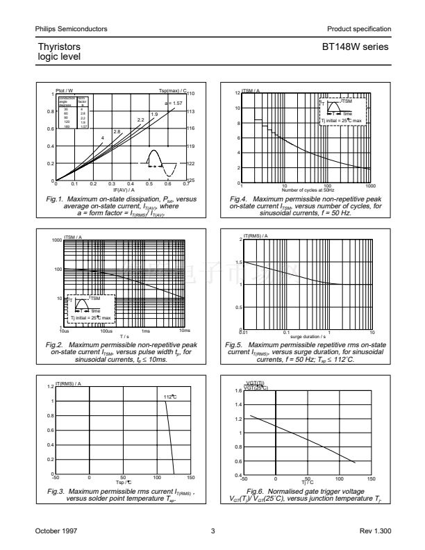 3
3
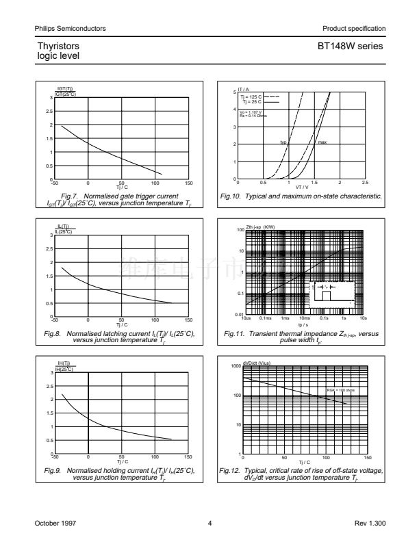 4
4
 5
5
 6
6
 7
7
