鈥?/div>
Pb鈭扚ree Packages are Available
225 mW Rating on FR鈭? or FR鈭? Board
Zener Breakdown Voltage Range 鈭?2.4 V to 75 V
Package Designed for Optimal Automated Board Assembly
Small Package Size for High Density Applications
ESD Rating of Class 3 (>16 KV) per Human Body Model
Tight Tolerance Series Available (See Page 4)
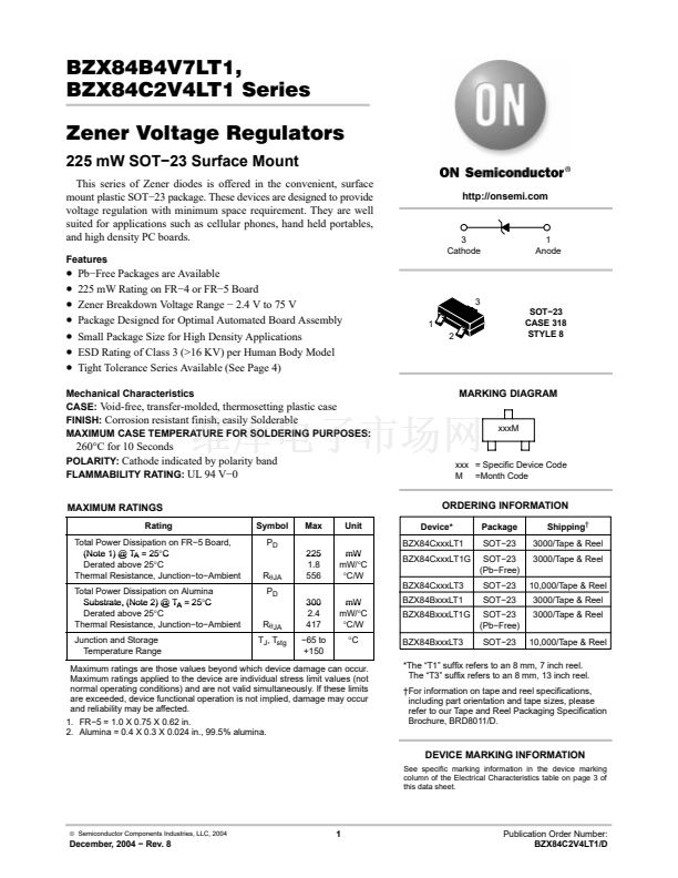
3
1
2
SOT鈭?3
CASE 318
STYLE 8
Mechanical Characteristics
CASE:
Void-free, transfer-molded, thermosetting plastic case
FINISH:
Corrosion resistant finish, easily Solderable
MAXIMUM CASE TEMPERATURE FOR SOLDERING PURPOSES:
MARKING DIAGRAM
xxxM
260掳C for 10 Seconds
POLARITY:
Cathode indicated by polarity band
FLAMMABILITY RATING:
UL 94 V鈭?
MAXIMUM RATINGS
Rating
Total Power Dissipation on FR鈭? Board,
(Note 1) @ T
A
= 25掳C
25 C
Derated above 25掳C
Thermal Resistance, Junction鈭抰o鈭扐mbient
Total Power Dissipation on Alumina
Substrate, (Note 2) @ T
A
= 25掳C
25 C
Derated above 25掳C
Thermal Resistance, Junction鈭抰o鈭扐mbient
Junction and Storage
Temperature Range
Symbol
P
D
225
1.8
556
300
2.4
417
鈭?5 to
+150
mW
mW/掳C
掳C/W
mW
mW/掳C
掳C/W
掳C
Max
Unit
xxx = Specific Device Code
M =Month Code
ORDERING INFORMATION
Device*
BZX84CxxxLT1
BZX84CxxxLT1G
BZX84CxxxLT3
BZX84BxxxLT1
BZX84BxxxLT1G
BZX84BxxxLT3
Package
SOT鈭?3
SOT鈭?3
(Pb鈭扚ree)
SOT鈭?3
SOT鈭?3
SOT鈭?3
(Pb鈭扚ree)
SOT鈭?3
Shipping
鈥?/div>
3000/Tape & Reel
3000/Tape & Reel
10,000/Tape & Reel
3000/Tape & Reel
3000/Tape & Reel
10,000/Tape & Reel
R
qJA
P
D
R
qJA
T
J
, T
stg
Maximum ratings are those values beyond which device damage can occur.
Maximum ratings applied to the device are individual stress limit values (not
normal operating conditions) and are not valid simultaneously. If these limits
are exceeded, device functional operation is not implied, damage may occur
and reliability may be affected.
1. FR鈭? = 1.0 X 0.75 X 0.62 in.
2. Alumina = 0.4 X 0.3 X 0.024 in., 99.5% alumina.
*The 鈥淭1鈥?suffix refers to an 8 mm, 7 inch reel.
The 鈥淭3鈥?suffix refers to an 8 mm, 13 inch reel.
鈥燜or information on tape and reel specifications,
including part orientation and tape sizes, please
refer to our Tape and Reel Packaging Specification
Brochure, BRD8011/D.
DEVICE MARKING INFORMATION
See specific marking information in the device marking
column of the Electrical Characteristics table on page 3 of
this data sheet.
漏
Semiconductor Components Industries, LLC, 2004
1
December, 2004 鈭?Rev. 8
Publication Order Number:
BZX84C2V4LT1/D


 1
1
 2
2
 3
3
 4
4
 5
5
 6
6
 7
7
 8
8
