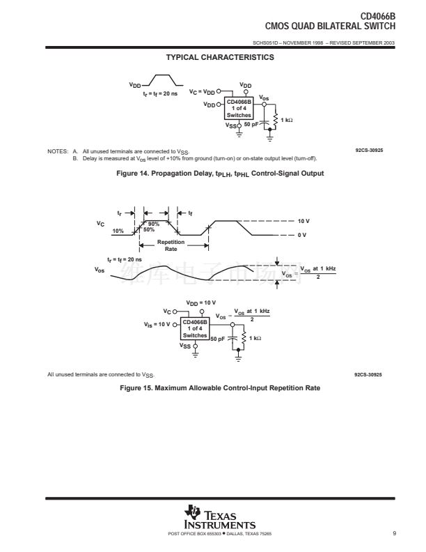
= 1 k鈩?/div>
D
D
D
D
D
D
Matched Control-Input to Signal-Output
Capacitance: Reduces Output Signal
Transients
Frequency Response, Switch On = 40 MHz
Typical
100% Tested for Quiescent Current at 20 V
5-V, 10-V, and 15-V Parametric Ratings
Meets All Requirements of JEDEC Tentative
Standard No. 13-B,
Standard Specifications
for Description of 鈥淏鈥?Series CMOS
Devices
Applications:
鈥?Analog Signal Switching/Multiplexing:
Signal Gating, Modulator, Squelch
Control, Demodulator, Chopper,
Commutating Switch
鈥?Digital Signal Switching/Multiplexing
鈥?Transmission-Gate Logic Implementation
鈥?Analog-to-Digital and Digital-to-Analog
Conversion
鈥?Digital Control of Frequency, Impedance,
Phase, and Analog-Signal Gain
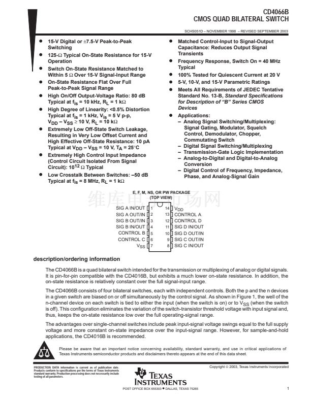
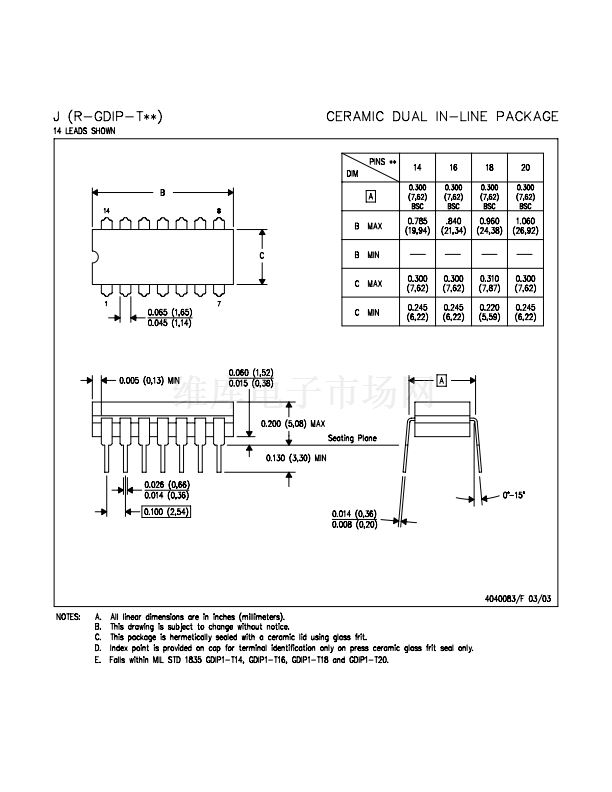
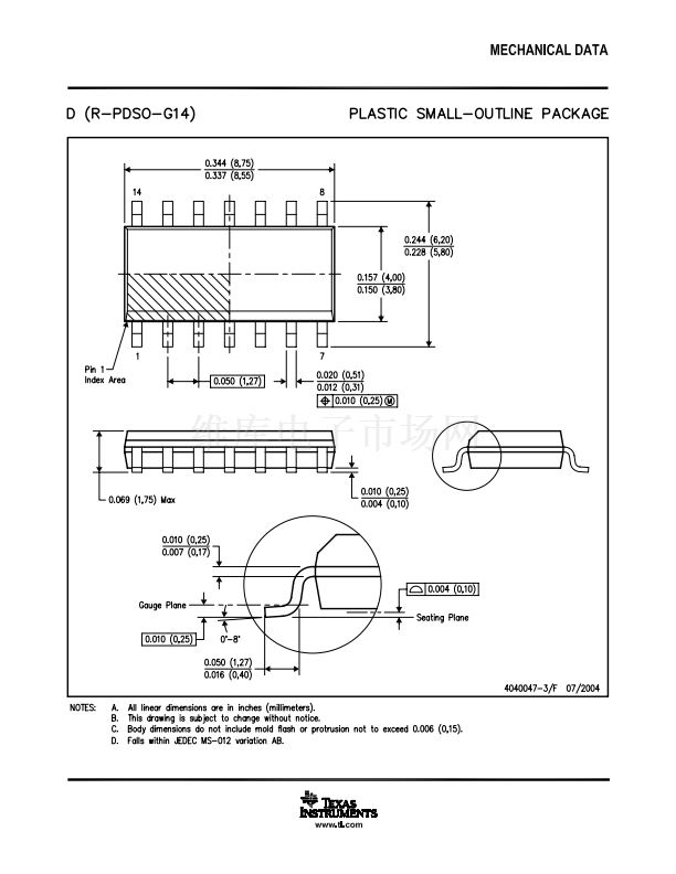
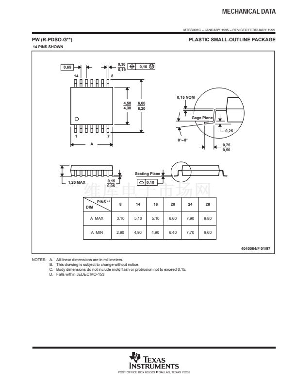
E, F, M, NS, OR PW PACKAGE
(TOP VIEW)
SIG A IN/OUT
SIG A OUT/IN
SIG B OUT/IN
SIG B IN/OUT
CONTROL B
CONTROL C
V
SS
1
2
3
4
5
6
7
14
13
12
11
10
9
8
V
DD
CONTROL A
CONTROL D
SIG D IN/OUT
SIG D OUT/IN
SIG C OUT/IN
SIG C IN/OUT
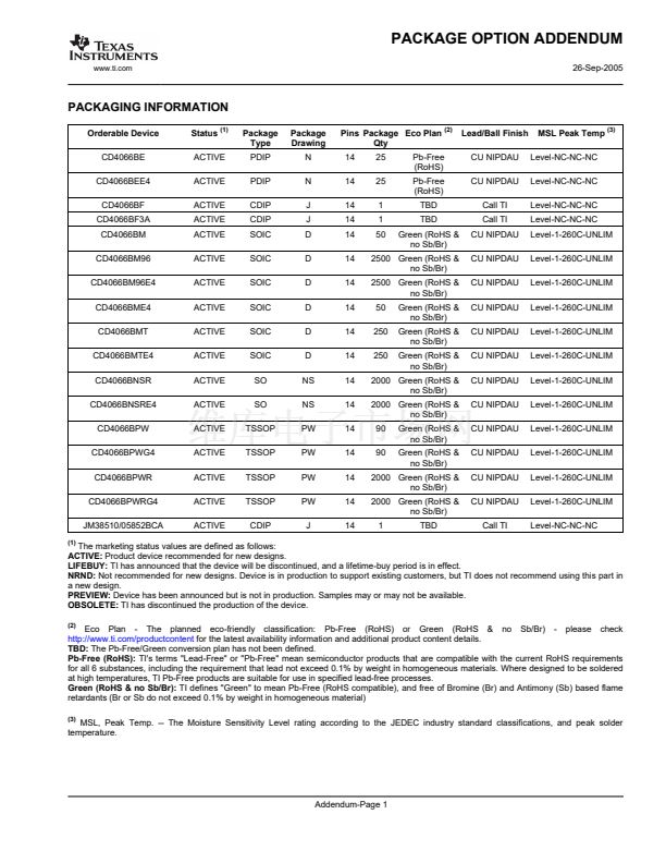
description/ordering information
The CD4066B is a quad bilateral switch intended for the transmission or multiplexing of analog or digital signals.
It is pin-for-pin compatible with the CD4016B, but exhibits a much lower on-state resistance. In addition, the
on-state resistance is relatively constant over the full signal-input range.
The CD4066B consists of four bilateral switches, each with independent controls. Both the p and the n devices
in a given switch are biased on or off simultaneously by the control signal. As shown in Figure 1, the well of the
n-channel device on each switch is tied to either the input (when the switch is on) or to V
SS
(when the switch
is off). This configuration eliminates the variation of the switch-transistor threshold voltage with input signal and,
thus, keeps the on-state resistance low over the full operating-signal range.
The advantages over single-channel switches include peak input-signal voltage swings equal to the full supply
voltage and more constant on-state impedance over the input-signal range. However, for sample-and-hold
applications, the CD4016B is recommended.
Please be aware that an important notice concerning availability, standard warranty, and use in critical applications of
Texas Instruments semiconductor products and disclaimers thereto appears at the end of this data sheet.
Copyright
铮?/div>
2003, Texas Instruments Incorporated
PRODUCTION DATA information is current as of publication date.
Products conform to specifications per the terms of Texas Instruments
standard warranty. Production processing does not necessarily include
testing of all parameters.
POST OFFICE BOX 655303
鈥?/div>
DALLAS, TEXAS 75265
1


 1
1
 2
2
 3
3
 4
4
 5
5
 6
6
 7
7
 8
8
 9
9
 10
10
 11
11
 12
12
 13
13
 14
14
 15
15
 16
16
 17
17
 18
18
 19
19
 20
20
