鈩?/div>
@V
GS
= 10V.
Super high dense cell design for extremely low R
DS(ON)
.
High power and current handing capability.
Lead free product is acquired.
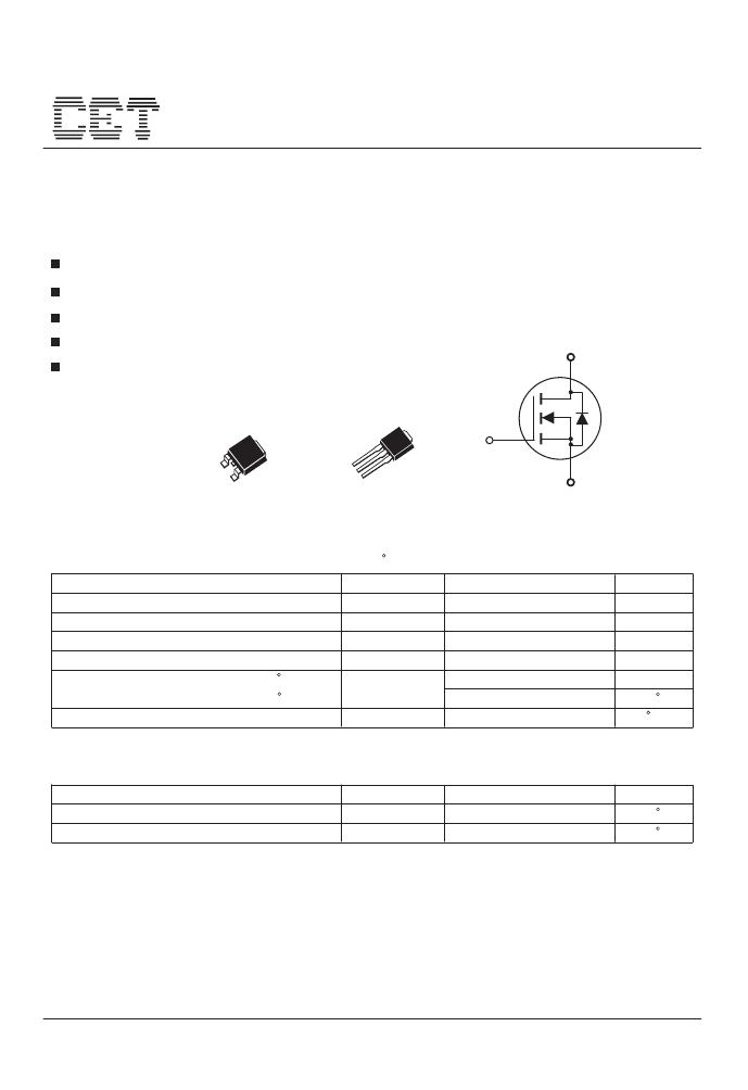
TO-251 & TO-252 package.
D
D
G
S
CEU SERIES
TO-252(D-PAK)
G
D
G
S
CED SERIES
TO-251(I-PAK)
S
ABSOLUTE MAXIMUM RATINGS
Parameter
Drain-Source Voltage
Gate-Source Voltage
Drain Current-Continuous
Drain Current-Pulsed
a
Tc = 25 C unless otherwise noted
Symbol
V
DS
V
GS
I
D
I
DM
P
D
T
J
,T
stg
Limit
650
Units
V
V
A
A
W
W/ C
C
卤
30
1.3
3.9
35
0.29
-55 to 150
Maximum Power Dissipation @ T
C
= 25 C
- Derate above 25 C
Operating and Store Temperature Range
Thermal Characteristics
Parameter
Thermal Resistance, Junction-to-Case
Thermal Resistance, Junction-to-Ambient
Symbol
R
胃JC
R
胃JA
Limit
3.5
50
Units
W/ C
W/ C
2005.July
6-6
http://www.cetsemi.com


 1
1
 2
2
 3
3
 4
4
