CY74FCT399T
QUAD 2-INPUT REGISTER
SCCS024A 鈥?MARCH 1994 鈥?REVISED OCTOBER 2001
D
D
D
D
D
D
D
D
Function, Pinout, and Drive Compatible
With FCT and F Logic
Reduced V
OH
(Typically = 3.3 V) Versions of
Equivalent FCT Functions
Edge-Rate Control Circuitry for
Significantly Improved Noise
Characteristics
I
off
Supports Partial-Power-Down Mode
Operation
Matched Rise and Fall Times
ESD Protection Exceeds JESD 22
鈥?2000-V Human-Body Model (A114-A)
鈥?200-V Machine Model (A115-A)
鈥?1000-V Charged-Device Model (C101)
Fully Compatible With TTL Input and
Output Logic Levels
64-mA Output Sink Current
32-mA Output Source Current
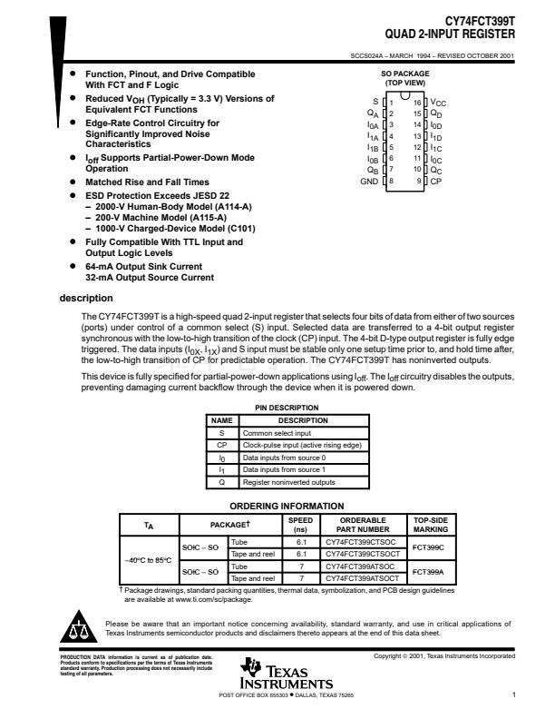
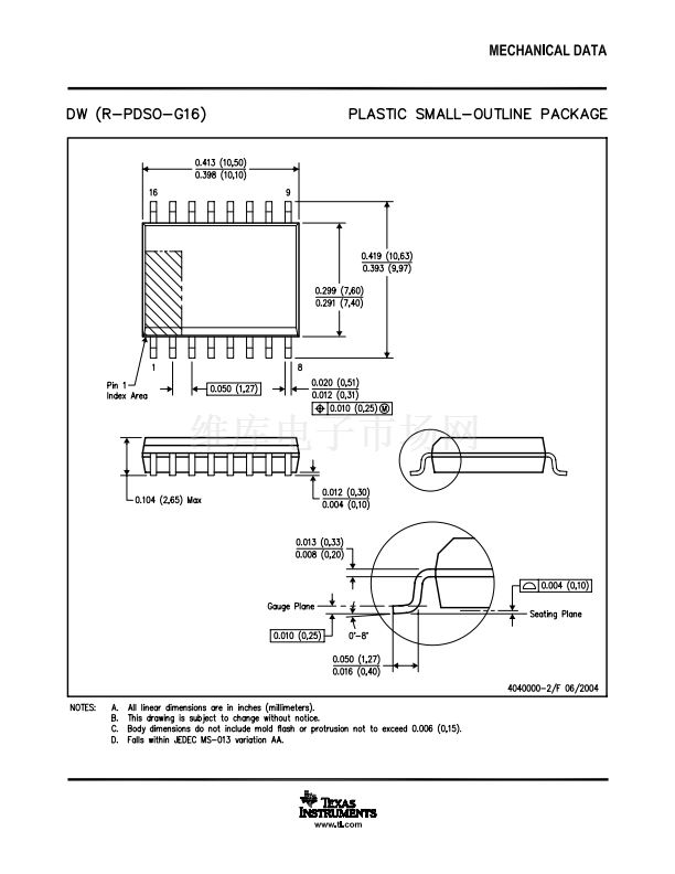
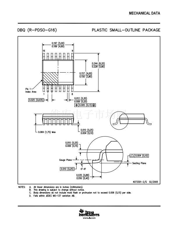
SO PACKAGE
(TOP VIEW)
S
Q
A
I
0A
I
1A
I
1B
I
0B
Q
B
GND
1
2
3
4
5
6
7
8
16
15
14
13
12
11
10
9
V
CC
Q
D
I
0D
I
1D
I
1C
I
0C
Q
C
CP
description
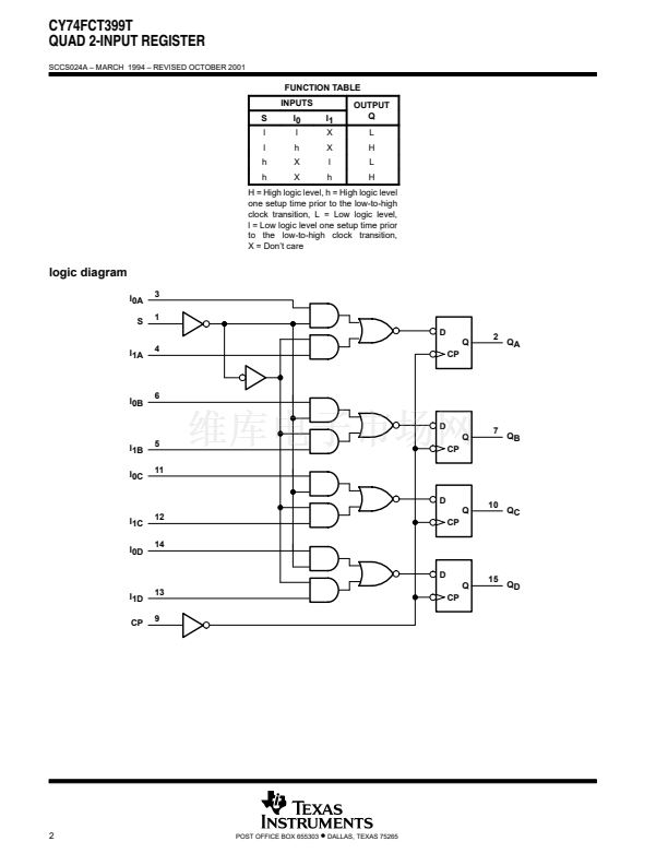
The CY74FCT399T is a high-speed quad 2-input register that selects four bits of data from either of two sources
(ports) under control of a common select (S) input. Selected data are transferred to a 4-bit output register
synchronous with the low-to-high transition of the clock (CP) input. The 4-bit D-type output register is fully edge
triggered. The data inputs (I
0X
, I
1X
) and S input must be stable only one setup time prior to, and hold time after,
the low-to-high transition of CP for predictable operation. The CY74FCT399T has noninverted outputs.
This device is fully specified for partial-power-down applications using I
off
. The I
off
circuitry disables the outputs,
preventing damaging current backflow through the device when it is powered down.
PIN DESCRIPTION
NAME
S
CP
I0
I1
Q
DESCRIPTION
Common select input
Clock-pulse input (active rising edge)
Data inputs from source 0
Data inputs from source 1
Register noninverted outputs
ORDERING INFORMATION
TA
PACKAGE鈥?/div>
SOIC 鈥?SO
鈥?0掳C to 85掳C
40掳C
SOIC 鈥?SO
Tube
Tape and reel
Tube
Tape and reel
SPEED
(ns)
6.1
6.1
7
7
ORDERABLE
PART NUMBER
CY74FCT399CTSOC
CY74FCT399CTSOCT
CY74FCT399ATSOC
CY74FCT399ATSOCT
TOP-SIDE
MARKING
FCT399C
FCT399A
鈥?Package drawings, standard packing quantities, thermal data, symbolization, and PCB design guidelines
are available at www.ti.com/sc/package.
Please be aware that an important notice concerning availability, standard warranty, and use in critical applications of
Texas Instruments semiconductor products and disclaimers thereto appears at the end of this data sheet.
Copyright
铮?/div>
2001, Texas Instruments Incorporated
PRODUCTION DATA information is current as of publication date.
Products conform to specifications per the terms of Texas Instruments
standard warranty. Production processing does not necessarily include
testing of all parameters.
POST OFFICE BOX 655303
鈥?/div>
DALLAS, TEXAS 75265
1


 1
1
 2
2
 3
3
 4
4
 5
5
 6
6
 7
7
 8
8
 9
9
 10
10
