鈻?/div>
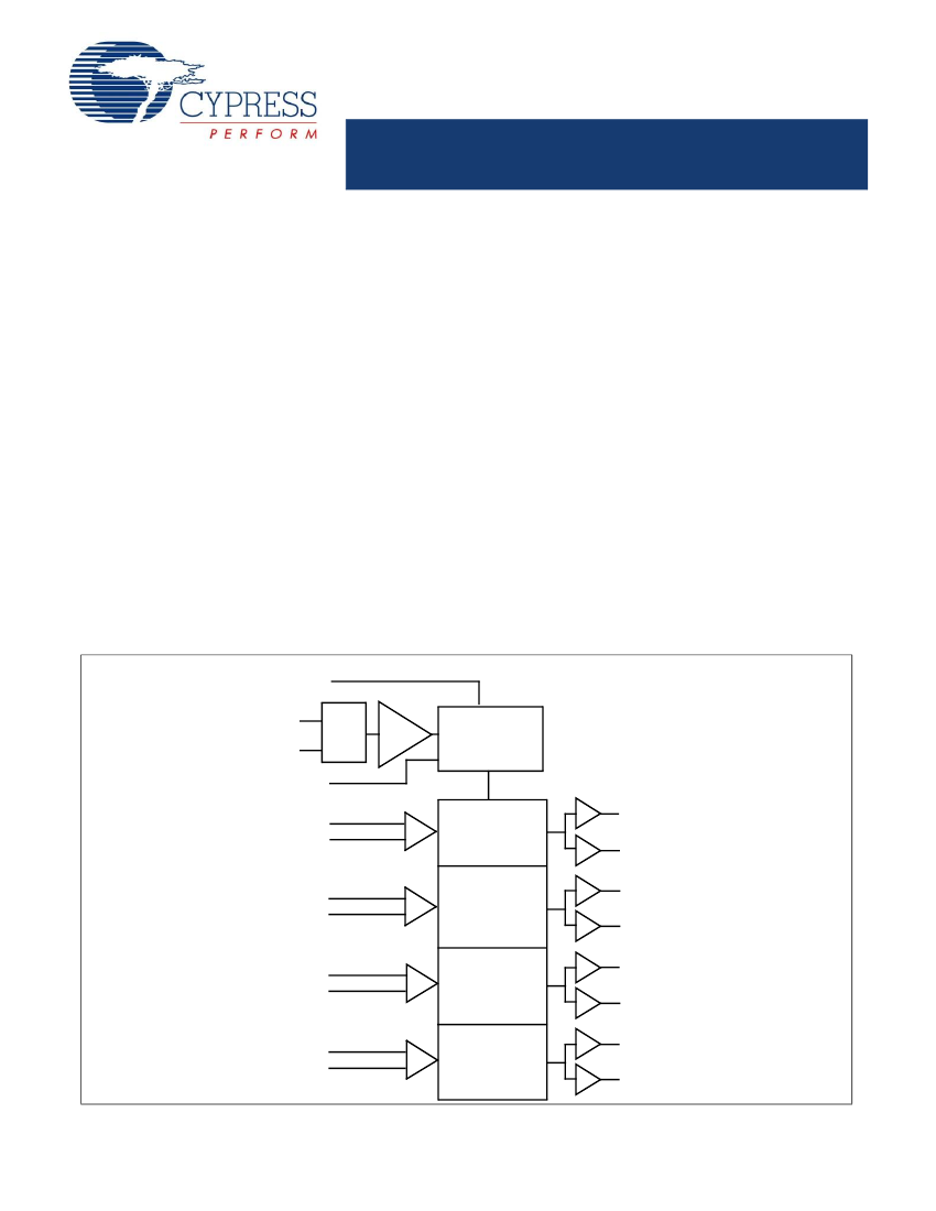
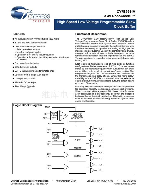
Functional Description
The CY7B9911V 3.3V RoboClock+鈩?High Speed Low
Voltage Programmable Skew Clock Buffer (LVPSCB) offers
user selectable control over system clock functions. These
multiple output clock drivers provide the system integrator with
functions necessary to optimize the timing of high perfor-
mance computer systems. Each of the eight individual drivers,
arranged in four pairs of user controllable outputs, can drive
terminated transmission lines with impedances as low as 50惟.
They deliver minimal and specified output skews and full swing logic
levels (LVTTL).
Each output is hardwired to one of nine delay or function
configurations. Delay increments of 0.7 to 1.5 ns are deter-
mined by the operating frequency with outputs that can skew
up to 卤6 time units from their nominal 鈥渮ero鈥?skew position. The
completely integrated PLL allows external load and cancels
the transmission line delay effects. When this 鈥渮ero delay鈥?/div>
capability of the LVPSCB is combined with the selectable
output skew functions, you can create output-to-output delays
of up to 卤12 time units.
Divide-by-two and divide-by-four output functions are provided
for additional flexibility in designing complex clock systems.
When combined with the internal PLL, these divide functions
allow distribution of a low frequency clock that are multiplied
by two or four at the clock destination. This facility minimizes
clock distribution difficulty enabling maximum system clock
speed and flexibility.
TEST
PHASE
FREQ
DET
FS
4F0
4F1
4Q0
SELECT
INPUTS
(THREE
LEVEL)
4Q1
SKEW
3Q0
3Q1
SELECT
2F0
2F1
2Q0
MATRIX
2Q1
1Q0
1Q1
All output pair skew <100 ps typical (250 max)
3.75 to 110 MHz output operation
User selectable output functions
鉂?/div>
Selectable skew to 18 ns
鉂?/div>
Inverted and non-inverted
1
1
鉂?/div>
Operation at
鈦?/div>
2
and
鈦?/div>
4
input frequency
鉂?/div>
Operation at 2x and 4x input frequency (input as low as
3.75 MHz)
Zero input-to-output delay
50% duty cycle outputs
LVTTL outputs drive 50惟 terminated lines
Operates from a single 3.3V supply
Low operating current
32-pin PLCC package
Jitter 100 ps (typical)
鈻?/div>
鈻?/div>
鈻?/div>
鈻?/div>
鈻?/div>
鈻?/div>
鈻?/div>
Logic Block Diagram
FB
REF
FILTER
VCO AND
TIME UNIT
GENERATOR
3F0
3F1
1F0
1F1
Cypress Semiconductor Corporation
Document Number: 38-07408 Rev. *D
鈥?/div>
198 Champion Court
鈥?/div>
San Jose
,
CA 95134-1709
鈥?/div>
408-943-2600
Revised June 20, 2007
CY7B9911V-7JXCT PDF文件相关型号
CY7B991V–2JC,CY7B991V–2JCT,CY7B991V–2JXC,CY7B991V–5JC,CY7B991V–5JCT,CY7B991V–5JIT,CY7B991V–5JXC,CY7B991V–5JXCT,CY7B991V–5JXI,CY7B991V–5JXIT,CY7B991V–7JC,CY7B991V–7JCT,CY7B991V–7JXC
CY7B9911V-7JXCT相关型号PDF文件下载
-
型号
版本
描述
厂商
下载
-
英文版
Industrial Control IC
ETC
-
英文版
Industrial Control IC
-
英文版
Industrial Control IC
ETC
-
英文版
Industrial Control IC
-
英文版
Industrial Control IC
ETC
-
英文版
Industrial Control IC
-
英文版
Industrial Control IC
ETC
-
英文版
Industrial Control IC
-
英文版
1Kx8 Dual-Port Static RAM
CYPRESS
-
英文版
1Kx8 Dual-Port Static RAM
CYPRESS [C...
-
英文版
4K x 8 Dual-Port Static RAMs and 4K x 8 Dual-Port Static RAM...
CYPRESS
-
英文版
4K x 8 Dual-Port Static RAMs and 4K x 8 Dual-Port Static RAM...
CYPRESS [C...
-
英文版
4K x 8 Dual-Port Static RAMs and 4K x 8 Dual-Port Static RAM...
CYPRESS
-
英文版
4K x 8 Dual-Port Static RAMs and 4K x 8 Dual-Port Static RAM...
CYPRESS [C...
-
英文版
4K x 8 Dual-Port Static RAMs and 4K x 8 Dual-Port Static RAM...
CYPRESS
-
英文版
4K x 8 Dual-Port Static RAMs and 4K x 8 Dual-Port Static RAM...
CYPRESS [C...
-
英文版
4K x8/9 Dual-Port Static RAM with Sem, Int, Busy
CYPRESS
-
英文版
4K x8/9 Dual-Port Static RAM with Sem, Int, Busy
CYPRESS [C...
-
英文版
4K x8/9 Dual-Port Static RAM with Sem, Int, Busy
CYPRESS
-
英文版
4K x8/9 Dual-Port Static RAM with Sem, Int, Busy
CYPRESS [C...


 1
1
 2
2
 3
3
 4
4
 5
5
 6
6
 7
7
 8
8
 9
9
 10
10
 11
11
 12
12
 13
13
 14
14
