DM74S299 3-STATE 8-Bit Universal Shift/Storage Register
August 1986
Revised May 2000
DM74S299
3-STATE 8-Bit Universal Shift/Storage Register
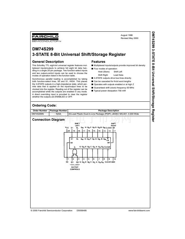
General Description
This Schottky TTL eight-bit universal register features mul-
tiplexed inputs/outputs to achieve full eight bit data han-
dling in a single 20-pin package. Two function-select inputs
and two output-control inputs can be used to choose the
modes of operation listed in the function table.
Synchronous parallel loading is accomplished by taking
both function-select lines, S0 and S1, HIGH. This places
the 3-STATE outputs in a high-impedance state, which per-
mits data that is applied on the input/output lines to be
clocked into the register. Reading out of the register can be
accomplished while the outputs are enabled in any mode.
A direct overriding input is provided to clear the register
whether the outputs are ENABLED or OFF.
Features
s
Multiplexed inputs/outputs provide improved bit density
s
Four modes of operation:
Hold (Store)
Shift Right
Shift Left
Load Data
s
3-STATE outputs drive bus lines directly
s
Can be cascaded for N-bit word lengths
s
Operates with outputs enabled or at high Z
s
Guaranteed shift (clock) frequency 50 MHz
s
Typical power dissipation 700 mW
Ordering Code:
Order Number
DM74S299N
Package Number
N20A
Package Description
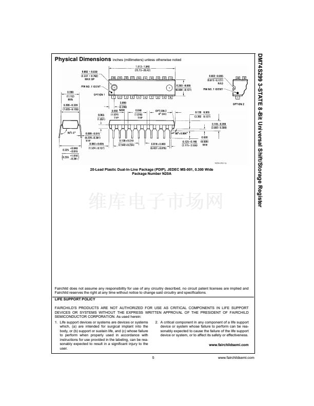
20-Lead Plastic Dual-In-Line Package (PDIP), JEDEC MS-001, 0.300 Wide
Connection Diagram
漏 2000 Fairchild Semiconductor Corporation
DS006485
www.fairchildsemi.com


 1
1
 2
2
 3
3
 4
4
 5
5
