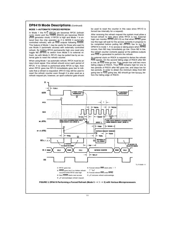
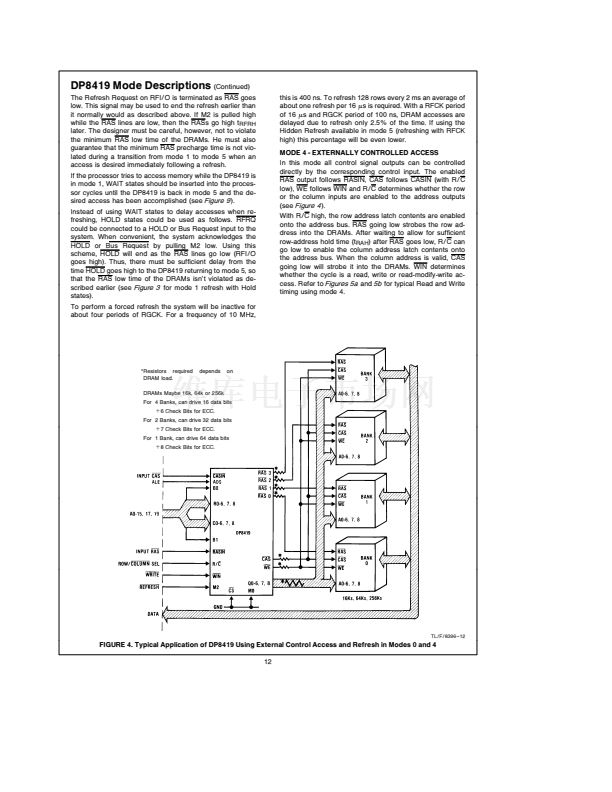
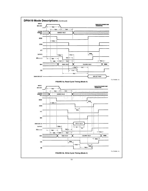
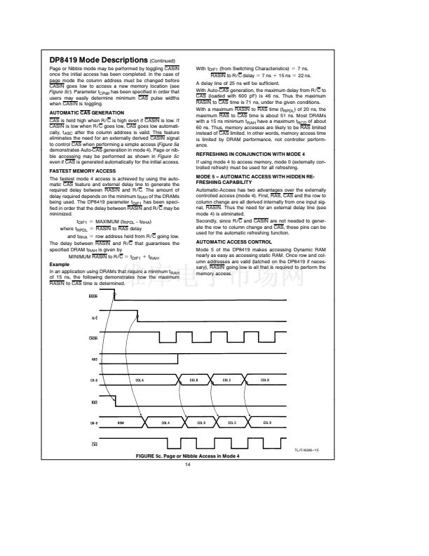
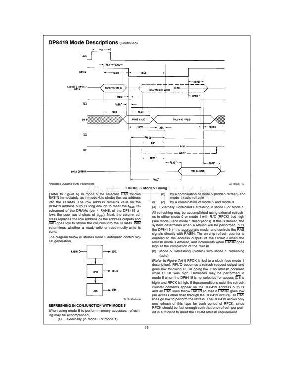
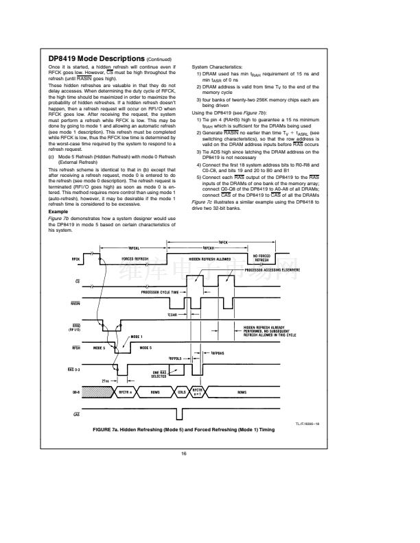
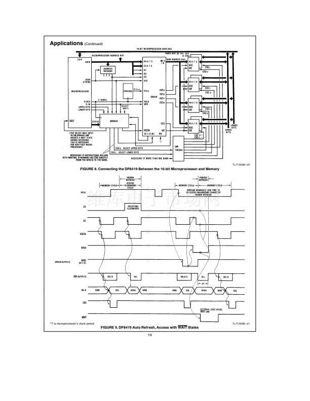
DP8417 NS32817 8418 32818 8419 32819 8419X 32819X 64k 256k Dynamic RAM
Controller Drivers
PRELIMINARY
August 1989
DP8417 NS32817 8418 32818 8419 32819 8419X
32819X 64k 256k Dynamic RAM Controller Drivers
General Description
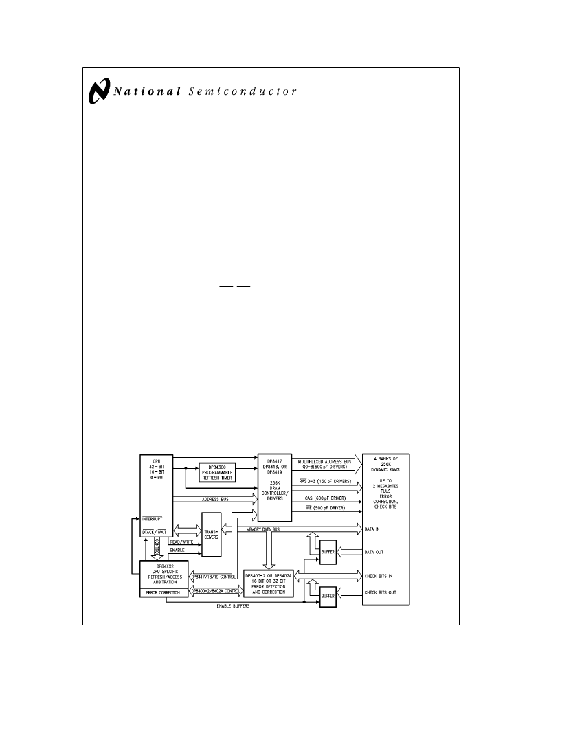
The DP8417 8418 8419 8419X represent a family of 256k
DRAM Controller Drivers which are designed to provide
鈥樷€楴o-Waitstate鈥欌€?CPU interface to Dynamic RAM arrays of up
to 2 Mbytes and larger Each device offers slight functional
variations of the DP8419 design which are tailored for differ-
ent system requirements All family members are fabricated
using National鈥檚 new oxide isolated Advanced Low power
Schottky (ALS) process and use design techniques which
enable them to significantly out-perform all other LSI or dis-
crete alternatives in speed level of integration and power
consumption
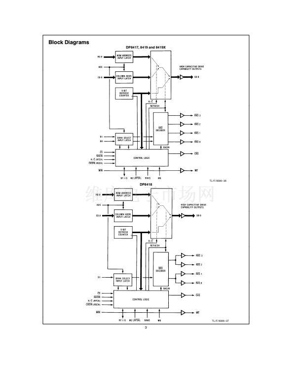
Each device integrates the following critical 256k DRAM
controller functions on a single monolithic device ultra pre-
cise delay line 9-bit refresh counter fall-through row col-
umn and bank select input latches Row Column address
muxing logic on-board high capacitive-load RAS CAS and
Write Enable Address output drivers and precise control
signal timing for all the above
There are four device options of the basic DP8419 Control-
ler The DP8417 is pin and function compatible with the
DP8419 except that its outputs are TRI-STATE
The
DP8418 changes one pin and is specifically designed to
offer an optimum interface to 32 bit microprocessors The
DP8419X is functionally identical to the DP8419 but is avail-
able in a 52-pin DIP package which is upward pin compati-
ble with National鈥檚 new DP8429D 1 Mbit DRAM Controller
Driver
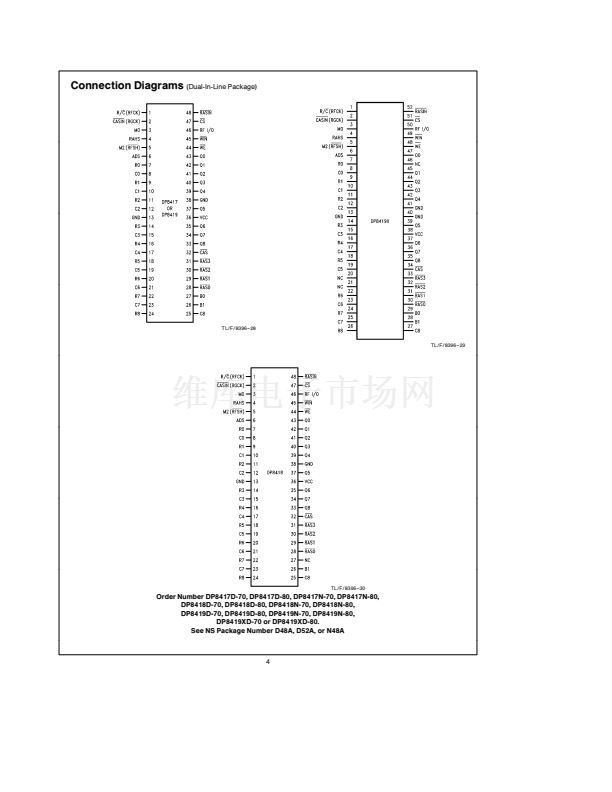
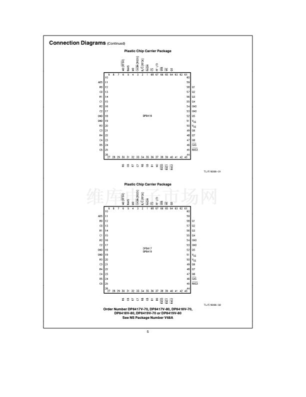
Each device is available in plastic DIP Ceramic DIP and
Plastic Chip Carrier (PCC) packaging (Continued)
TRI-STATE is a registered trademark of National Semiconductor Corp
PAL is a registered trademark of and used under license with Monolithic Memories Inc
Operational Features
Y
Y
Y
Y
Y
Y
Y
Y
Y
Y
Makes DRAM Interface and refresh tasks appear virtu-
ally transparent to the CPU making DRAMs as easy to
use as static RAMs
Specifically designed to eliminate CPU wait states up to
10 MHz or beyond
Eliminates 15 to 20 SSI MSI components for significant
board real estate reduction system power savings and
the elimination of chip-to-chip AC skewing
On-board ultra precise delay line
On-board high capacitive RAS CAS WE and address
drivers (specified driving 88 DRAMs directly)
AC specified for directly addressing up to 8 Megabytes
Low power high speed bipolar oxide isolated process
Upward pin and function compatible with new DP8428
DP8429 1 Mbit DRAM controller drivers
Downward pin and function compatible with DP8408A
DP8409A 64k 256k DRAM controller drivers
4 user selectable modes of operation for Access and
Refresh (2 automatic 2 external)
Contents
Y
Y
Y
Y
Y
Y
Y
System and Device Block Diagrams
Recommended Companion Components
Device Connection Diagrams and Pin Definitions
Family Device Differences
(DP8419 vs DP8409A 8417 8418 8419X)
Mode of Operation
(Descriptions and Timing Diagrams)
Application Description and Diagrams
DC AC Electrical Specifications Timing Diagrams and
Test Conditions
System Diagram
TL F 8396 鈥?25
C
1995 National Semiconductor Corporation
TL F 8396
RRD-B30M105 Printed in U S A


 1
1
 2
2
 3
3
 4
4
 5
5
 6
6
 7
7
 8
8
 9
9
 10
10
 11
11
 12
12
 13
13
 14
14
 15
15
 16
16
 17
17
 18
18
 19
19
 20
20
 21
21
 22
22
 23
23
 24
24
 25
25
 26
26
 27
27
 28
28
