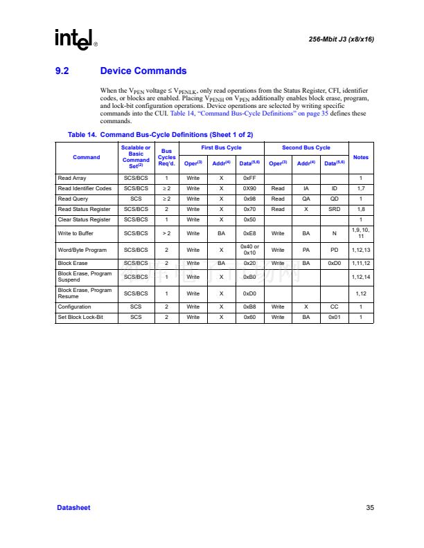
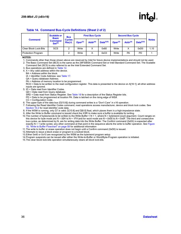
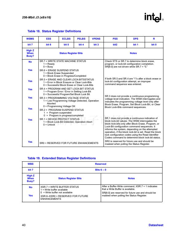
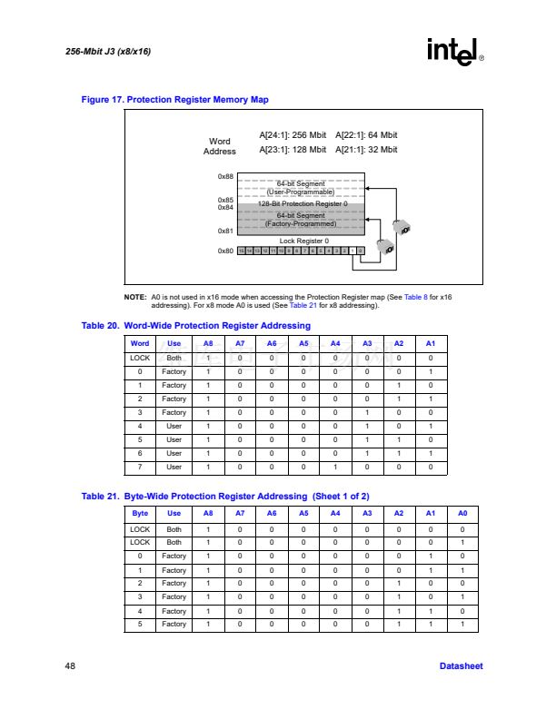
鈻?/div>
Architecture
鈥?Multi-Level Cell Technology: High
Density at Low Cost
鈥?High-Density Symmetrical 128-Kbyte
Blocks
鈥?56 Mbit (256 Blocks) (0.18碌m only)
鈥?28 Mbit (128 Blocks)
鈥?4 Mbit (64 Blocks)
鈥?2 Mbit (32 Blocks)
Quality and Reliability
鈥?Operating Temperature:
-40 掳C to +85 掳C
鈥?100K Minimum Erase Cycles per Block
鈥?0.18 碌m ETOX鈩?VII Process (J3C)
鈥?0.25 碌m ETOX鈩?VI Process (J3A)
Packaging and Voltage
鈥?56-Lead TSOP Package
鈥?64-Ball Intel
庐
Easy BGA Package
鈥?Lead-free packages available
鈥?48-Ball Intel
庐
VF BGA Package (32 and
64 Mbit) (x16 only)
鈥?V
CC
=
2.7 V to 3.6 V
鈥?V
CCQ
= 2.7 V to 3.6 V
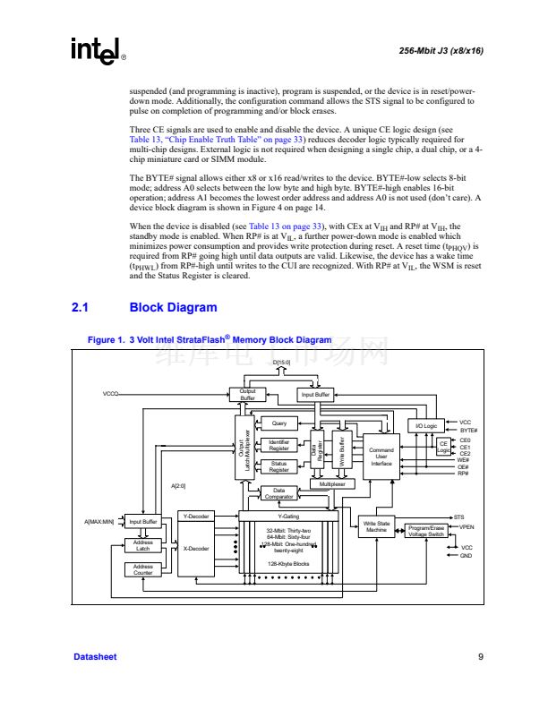
Capitalizing on Intel鈥檚 0.25 and 0.18 micron, two-bit-per-cell technology, the Intel StrataFlash
庐
Memory (J3)
device provides 2X the bits in 1X the space, with new features for mainstream performance. Offered in 256-
Mbit (32-Mbyte), 128-Mbit (16-Mbyte), 64-Mbit, and 32-Mbit densities, the J3 device brings reliable, two-bit-
per-cell storage technology to the flash market segment. Benefits include more density in less space, high-speed
interface, lowest cost-per-bit NOR device, support for code and data storage, and easy migration to future
devices.
Using the same NOR-based ETOX鈩?technology as Intel鈥檚 one-bit-per-cell products, the J3 device takes
advantage of over one billion units of flash manufacturing experience since 1987. As a result, J3 components
are ideal for code and data applications where high density and low cost are required. Examples include
networking, telecommunications, digital set top boxes, audio recording, and digital imaging.
By applying FlashFile鈩?memory family pinouts, J3 memory components allow easy design migrations from
existing Word-Wide FlashFile memory (28F160S3 and 28F320S3), and first generation Intel StrataFlash
庐
memory (28F640J5 and 28F320J5) devices.
J3 memory components deliver a new generation of forward-compatible software support. By using the
Common Flash Interface (CFI) and the Scalable Command Set (SCS), customers can take advantage of density
upgrades and optimized write capabilities of future Intel StrataFlash
庐
memory devices. Manufactured on Intel
庐
0.18 micron ETOX鈩?VII (J3C) and 0.25 micron ETOX鈩?VI (J3A) process technology, the J3 memory device
provides the highest levels of quality and reliability.
Notice:
This document contains information on new products in production. The specifications are
subject to change without notice. Verify with your local Intel sales office that you have the latest
datasheet before finalizing a design.
Order Number: 290667-021
March 2005


 1
1
 2
2
 3
3
 4
4
 5
5
 6
6
 7
7
 8
8
 9
9
 10
10
 11
11
 12
12
 13
13
 14
14
 15
15
 16
16
 17
17
 18
18
 19
19
 20
20
 21
21
 22
22
 23
23
 24
24
 25
25
 26
26
 27
27
 28
28
 29
29
 30
30
 31
31
 32
32
 33
33
 34
34
 35
35
 36
36
 37
37
 38
38
 39
39
 40
40
 41
41
 42
42
 43
43
 44
44
 45
45
 46
46
 47
47
 48
48
 49
49
 50
50
 51
51
 52
52
 53
53
 54
54
 55
55
 56
56
 57
57
 58
58
 59
59
 60
60
 61
61
 62
62
 63
63
 64
64
 65
65
 66
66
 67
67
 68
68
 69
69
 70
70
 71
71
 72
72
