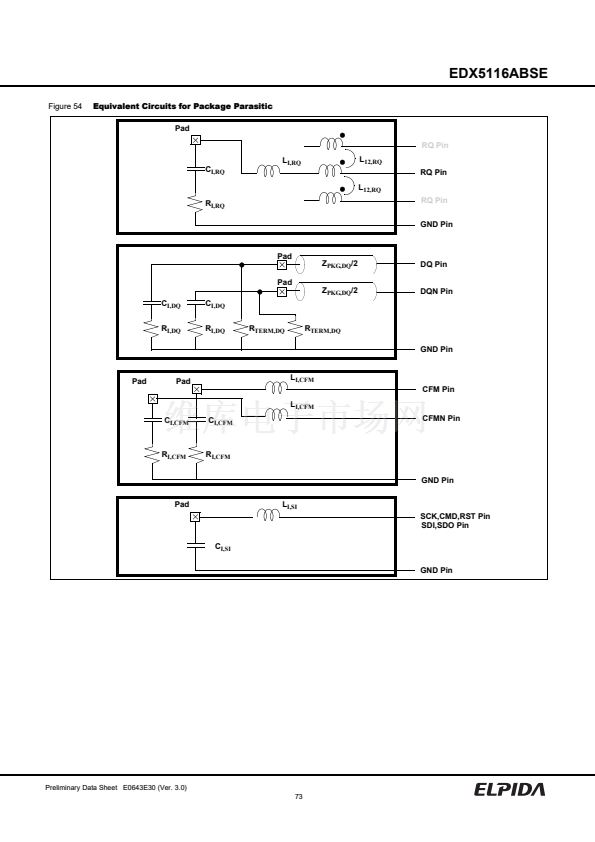
鈥?/div>
Highest pin bandwidth available
4000/3200/2400 Mb/s Octal Data Rate (ODR) Signaling
鈥?Bi-directional differential RSL (DRSL)
- Flexible read/write bandwidth allocation
- Minimum pin count
鈥?On-chip termination
-Adaptive impedance matching
-Reduced system cost and routing complexity
Highest sustained bandwidth per DRAM device
鈥?8000/6400/4800 MB/s sustained data rate
鈥?Eight banks: bank-interleaved transactions at full
bandwidth
鈥?Dynamic request scheduling
鈥?Early-read-after-write support for maximum efficiency
鈥?Zero overhead refresh
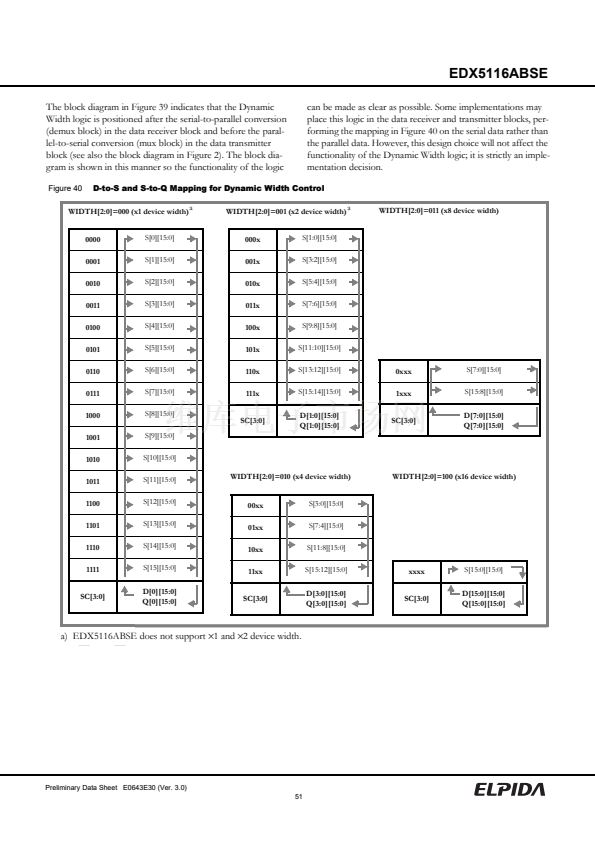
Dynamic width control
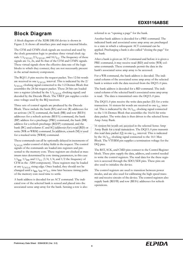
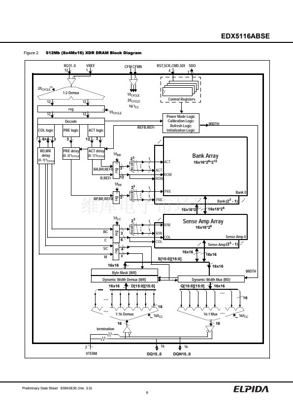
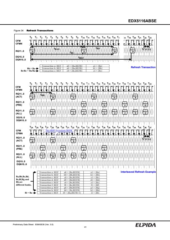
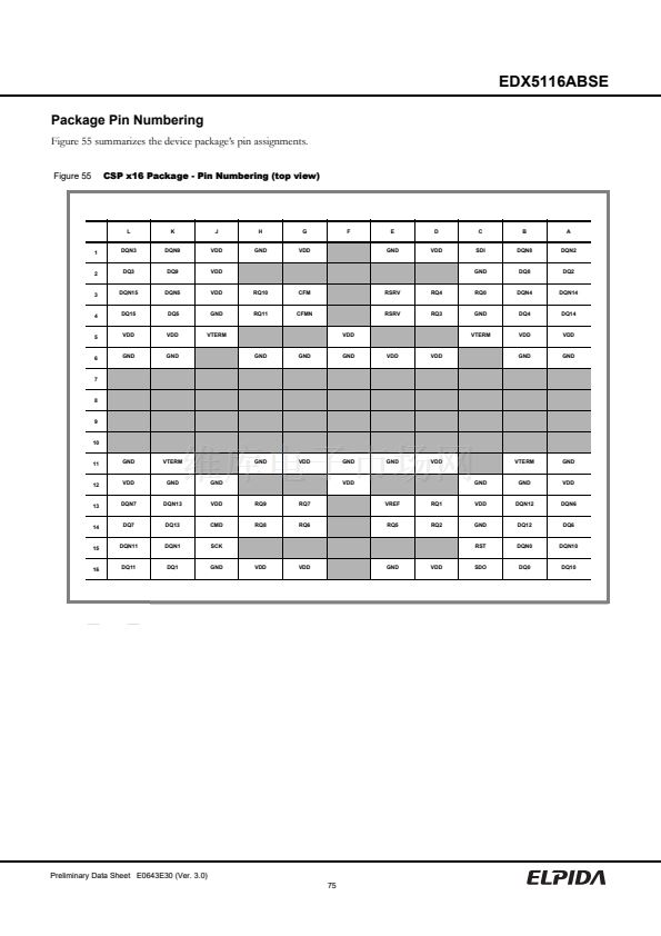
鈥DX5116ABSE supports
脳
16,
脳
8 and
脳
4 mode
Low latency
鈥?2.0/2.5/3.33 ns request packets
鈥?Point-to-point data interconnect for fastest possible
flight time
鈥?Support for low-latency, fast-cycle cores
11
12
13
14
15
16
GND
VDD
GND
RQ3
VDD
RQ1
VDD
VTERM GND
GND
GND
GND
VDD
GND
RST
GND GND
SD0
CMD
DQN13 VDD
RQ9
DQ0
DQN0
DQ13 CMD
RQ8
DQN7
DQ7
VREF
RQ5
SCK
RQ1
SD1
VDD DQN12 DQN6
DQ6
DQN2
DG2
RQ2
GND DQ12
VTERM
GND
VDD
DQN11 DQN1 SCK
DQ11
DQ4
DQN4
GND
DQ1
VDD
VDD
GND
GND
RST DQN0 DQN10
DQ10
DQN6
DQ6
VDD
SDO
DQ0
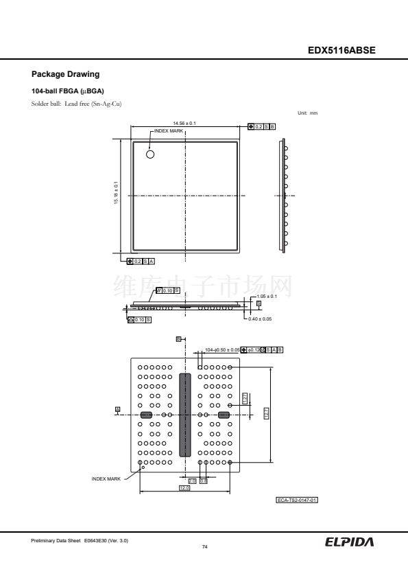
A16
A8
Top view of package
鈥?/div>
鈥?/div>
鈥?/div>
Doc. No. E0643E30 (Ver. 3.0)
Date Published August 2005 (K) Japan
Printed in Japan
URL: http://www.elpida.com
铮?/div>
Elpida Memory, Inc.
2005


 1
1
 2
2
 3
3
 4
4
 5
5
 6
6
 7
7
 8
8
 9
9
 10
10
 11
11
 12
12
 13
13
 14
14
 15
15
 16
16
 17
17
 18
18
 19
19
 20
20
 21
21
 22
22
 23
23
 24
24
 25
25
 26
26
 27
27
 28
28
 29
29
 30
30
 31
31
 32
32
 33
33
 34
34
 35
35
 36
36
 37
37
 38
38
 39
39
 40
40
 41
41
 42
42
 43
43
 44
44
 45
45
 46
46
 47
47
 48
48
 49
49
 50
50
 51
51
 52
52
 53
53
 54
54
 55
55
 56
56
 57
57
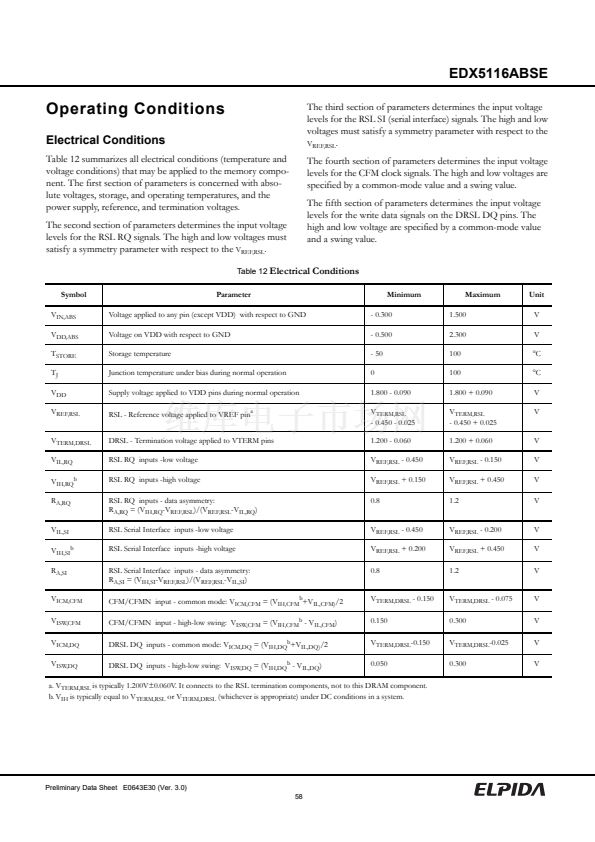 58
58
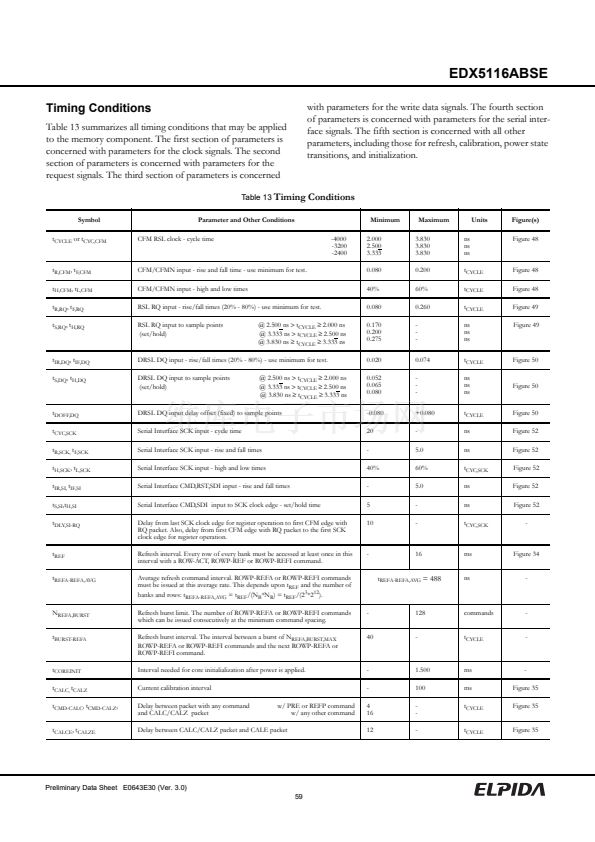 59
59
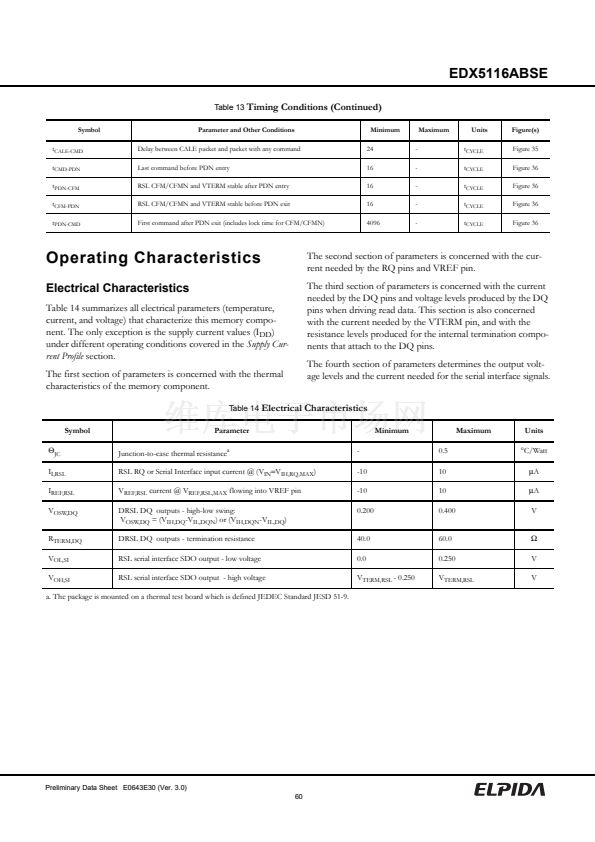 60
60
 61
61
 62
62
 63
63
 64
64
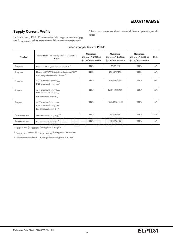
 65
65
 66
66
 67
67
 68
68
 69
69
 70
70
 71
71
 72
72
 73
73
 74
74
 75
75
 76
76
 77
77
 78
78
