Placement ef铿乧iency of Chip Resistor Array is two, four or eight times of the 铿俛t type chip resistor
鈻?/div>
Explanation of Part Numbers
1
2
3
4
5
6
7
8
9
10
11
E
X
B
V
8
V
4
7
2
J
V
Product Code
Thick Film
Chip Resistor
Networks
1
2
3
N
V
S
Chip Resistor Array
Type: inches
0201 Array
0402 Array
Convex Terminal
0603 Array
0402 Array
0603 Array Concave Terminal
0805 Array
No. of Terminal
4 4 Terminal
8 8 Terminal
H 16 Terminal
Schematics
V
Isolated
type
Resistance Value
The first two digits are
significant figures of
resistance value and
the third one denotes
the number of zeros
following. Jumper is
expressed by R00
Example: 222: 2.2 k
Resistance
Tolerance
J
卤5
%
0 Jumper
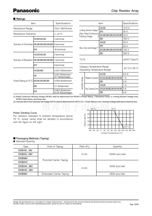
Packaging Methods
Packaging
Code
Nil
Embossed
Carrier Taping
(S8V)
Punched Carrier Taping
2 mm pitch
(14V, 18V, 24V, 28V, N8V)
Punched Carrier Taping
4 mm pitch
(2HV, 34V, 38V, V4V, V8V)
X
V
鈻?/div>
Construction (Example : Concave Terminal)
鈻?/div>
Schematics
鈼?/div>
Isolated type
14V, 24V, 34V, V4V
2 resistors
4
3
8
18V, 28V, N8V, 38V, V8V, S8V
4 resistors
7
6
5
Protective coating
1
2
1
2
3
4
Alumina substrate
Electrode (Outer)
Electrode (Between)
2HV
8 resistors
16 15 14 13 12 11 10
9
Thick film
resistive element
Electrode (Inner)
1
2
3
4
5
6
7
8
Design and speci铿乧ations are each subject to change without notice. Ask factory for the current technical speci铿乧ations before purchase and/or use.
Should a safety concern arise regarding this product, please be sure to contact us immediately.
May. 2005


 1
1
 2
2
 3
3
 4
4
 5
5
 6
6
