Impedance Matched Zin/Zout = 50鈩?/div>
Hermetically Sealed Package
DESCRIPTION
The FLM3742-25F is a power GaAs FET that is internally matched for
standard communication bands to provide optimum power and gain in
a 50 ohm system.
Eudyna鈥檚 stringent Quality Assurance Program assures the highest
reliability and consistent performance.
ABSOLUTE MAXIMUM RATING (Ambient Temperature Ta=25掳C)
Item
Drain-Source Voltage
Gate-Source Voltage
Total Power Dissipation
Storage Temperature
Channel Temperature
Symbol
VDS
VGS
PT
Tstg
Tch
Tc = 25掳C
Condition
Rating
15
-5
93.7
-65 to +175
175
Unit
V
V
W
掳C
掳C
Fujitsu recommends the following conditions for the reliable operation of GaAs FETs:
1. The drain-source operating voltage (VDS) should not exceed 10 volts.
2. The forward and reverse gate currents should not exceed 64.0 and -11.2 mA respectively with
gate resistance of 25鈩?
ELECTRICAL CHARACTERISTICS (Ambient Temperature Ta=25掳C)
Item
Saturated Drain Current
Transconductance
Pinch-off Voltage
Gate Source Breakdown Voltage
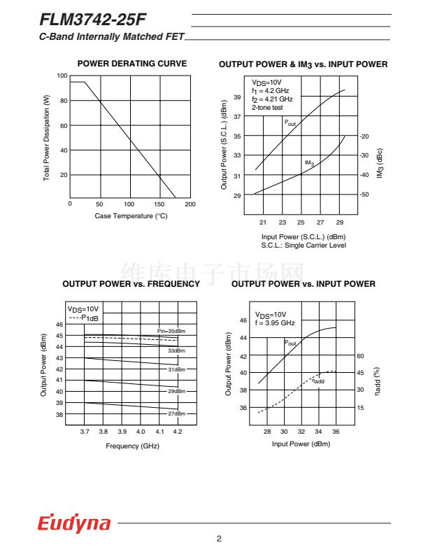
Output Power at 1dB G.C.P.
Power Gain at 1dB G.C.P.
Drain Current
Power-added Efficiency
Gain Flatness
3rd Order Intermodulation
Distortion
Thermal Resistance
Channel Temperature Rise
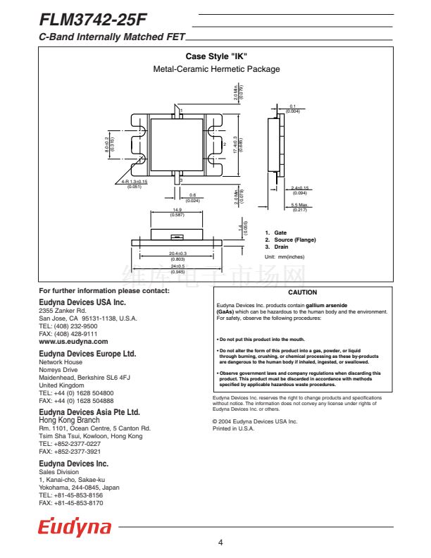
CASE STYLE:
IK
Symbol
IDSS
gm
Vp
VGSO
P1dB
G1dB
Idsr
畏
add
鈭咷
IM3
Rth
鈭員
ch
f = 4.2 GHz,
鈭唂
= 10 MHz
2-Tone Test
Pout = 33.5dBm S.C.L.
Channel to Case
10V x Idsr x Rth
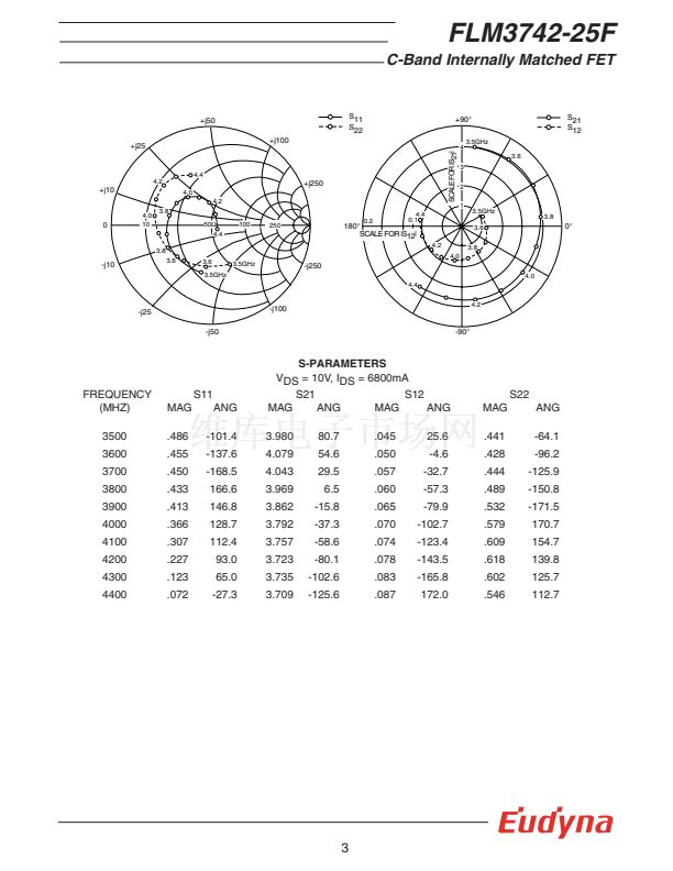
VDS =10V,
IDS = 0.55 IDSS (Typ.),
f = 3.7 ~ 4.2 GHz,
ZS=ZL= 50 ohm
Test Conditions
VDS = 5V, VGS = 0V
VDS = 5V, IDS = 6800mA
VDS = 5V, IDS = 600mA
IGS = -600碌A
Min.
-
-
-1.0
-5.0
43.5
9.5
-
-
-
-44
-
-
Limit
Typ. Max.
11.6 17.4
-
5800
-2.0
-
44.5
10.5
-3.5
-
-
-
Unit
A
mS
V
V
dBm
dB
mA
%
dB
dBc
掳C/W
掳C
6200 7600
41
-
-46
1.4
-
-
卤0.6
-
1.6
100
G.C.P.: Gain Compression Point, S.C.L.: Single Carrier Level
Edition 1.3
August 2004
1


 1
1
 2
2
 3
3
 4
4
