Semiconductor
HGTG20N120E2
34A, 1200V N-Channel IGBT
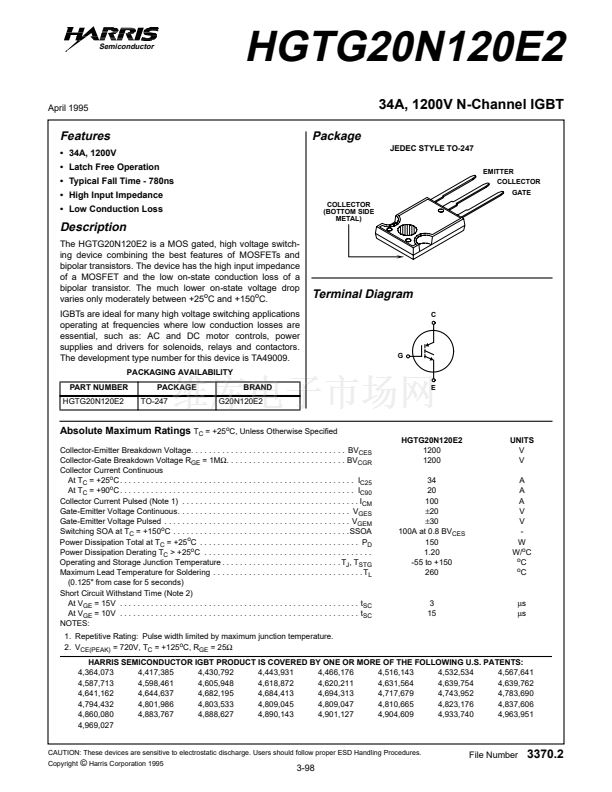
Package
JEDEC STYLE TO-247
EMITTER
COLLECTOR
GATE
COLLECTOR
(BOTTOM SIDE
METAL)
April 1995
Features
鈥?34A, 1200V
鈥?Latch Free Operation
鈥?Typical Fall Time - 780ns
鈥?High Input Impedance
鈥?Low Conduction Loss
Description
The HGTG20N120E2 is a MOS gated, high voltage switch-
ing device combining the best features of MOSFETs and
bipolar transistors. The device has the high input impedance
of a MOSFET and the low on-state conduction loss of a
bipolar transistor. The much lower on-state voltage drop
varies only moderately between +25
o
C and +150
o
C.
IGBTs are ideal for many high voltage switching applications
operating at frequencies where low conduction losses are
essential, such as: AC and DC motor controls, power
supplies and drivers for solenoids, relays and contactors.
The development type number for this device is TA49009.
PACKAGING AVAILABILITY
PART NUMBER
HGTG20N120E2
PACKAGE
TO-247
BRAND
G20N120E2
E
Terminal Diagram
C
G
Absolute Maximum Ratings
T
C
= +25
o
C, Unless Otherwise Speci铿乪d
Collector-Emitter Breakdown Voltage. . . . . . . . . . . . . . . . . . . . . . . . . . . . . . . . . . . BV
CES
Collector-Gate Breakdown Voltage R
GE
= 1M鈩? . . . . . . . . . . . . . . . . . . . . . . . . . . BV
CGR
Collector Current Continuous
At T
C
= +25
o
C. . . . . . . . . . . . . . . . . . . . . . . . . . . . . . . . . . . . . . . . . . . . . . . . . . . . . I
C25
At T
C
= +90
o
C. . . . . . . . . . . . . . . . . . . . . . . . . . . . . . . . . . . . . . . . . . . . . . . . . . . . . I
C90
Collector Current Pulsed (Note 1) . . . . . . . . . . . . . . . . . . . . . . . . . . . . . . . . . . . . . . . . I
CM
Gate-Emitter Voltage Continuous. . . . . . . . . . . . . . . . . . . . . . . . . . . . . . . . . . . . . . . V
GES
Gate-Emitter Voltage Pulsed . . . . . . . . . . . . . . . . . . . . . . . . . . . . . . . . . . . . . . . . . . V
GEM
Switching SOA at T
C
= +150
o
C . . . . . . . . . . . . . . . . . . . . . . . . . . . . . . . . . . . . . . . .SSOA
Power Dissipation Total at T
C
= +25
o
C . . . . . . . . . . . . . . . . . . . . . . . . . . . . . . . . . . . . P
D
Power Dissipation Derating T
C
> +25
o
C . . . . . . . . . . . . . . . . . . . . . . . . . . . . . . . . . . . . . .
Operating and Storage Junction Temperature . . . . . . . . . . . . . . . . . . . . . . . . . . . T
J
, T
STG
Maximum Lead Temperature for Soldering . . . . . . . . . . . . . . . . . . . . . . . . . . . . . . . . . . T
L
(0.125" from case for 5 seconds)
Short Circuit Withstand Time (Note 2)
At V
GE
= 15V . . . . . . . . . . . . . . . . . . . . . . . . . . . . . . . . . . . . . . . . . . . . . . . . . . . . . . t
SC
At V
GE
= 10V . . . . . . . . . . . . . . . . . . . . . . . . . . . . . . . . . . . . . . . . . . . . . . . . . . . . . . t
SC
NOTES:
1. Repetitive Rating: Pulse width limited by maximum junction temperature.
2. V
CE(PEAK)
= 720V, T
C
= +125
o
C, R
GE
= 25鈩?/div>
HGTG20N120E2
1200
1200
34
20
100
卤20
卤30
100A at 0.8 BV
CES
150
1.20
-55 to +150
260
UNITS
V
V
A
A
A
V
V
-
W
W/
o
C
o
C
o
C
3
15
碌s
碌s
HARRIS SEMICONDUCTOR IGBT PRODUCT IS COVERED BY ONE OR MORE OF THE FOLLOWING U.S. PATENTS:
4,364,073
4,417,385
4,430,792
4,443,931
4,466,176
4,516,143
4,532,534
4,567,641
4,587,713
4,598,461
4,605,948
4,618,872
4,620,211
4,631,564
4,639,754
4,639,762
4,641,162
4,644,637
4,682,195
4,684,413
4,694,313
4,717,679
4,743,952
4,783,690
4,794,432
4,801,986
4,803,533
4,809,045
4,809,047
4,810,665
4,823,176
4,837,606
4,860,080
4,883,767
4,888,627
4,890,143
4,901,127
4,904,609
4,933,740
4,963,951
4,969,027
CAUTION: These devices are sensitive to electrostatic discharge. Users should follow proper ESD Handling Procedures.
Copyright
漏
Harris Corporation 1995
File Number
3370.2
3-98


 1
1
 2
2
 3
3
 4
4
 5
5
