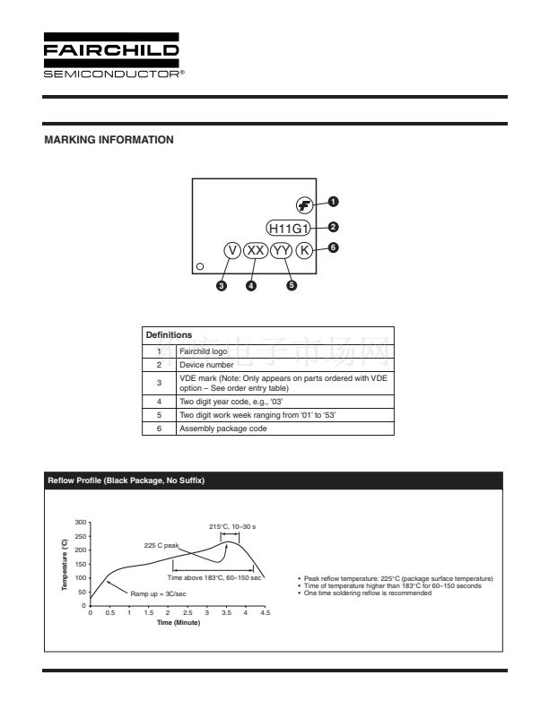
鈥?/div>
CMOS logic interface
Telephone ring detector
Low input TTL interface
Power supply isolation
Replace pulse transformer
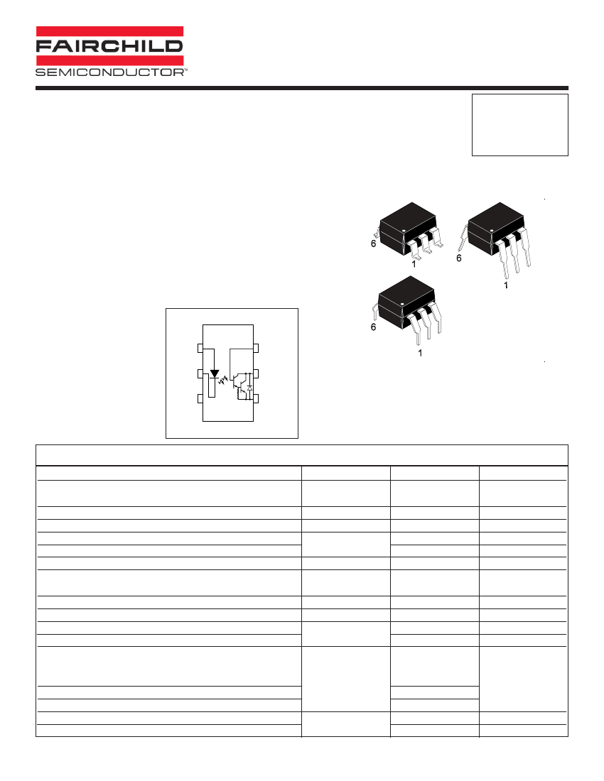
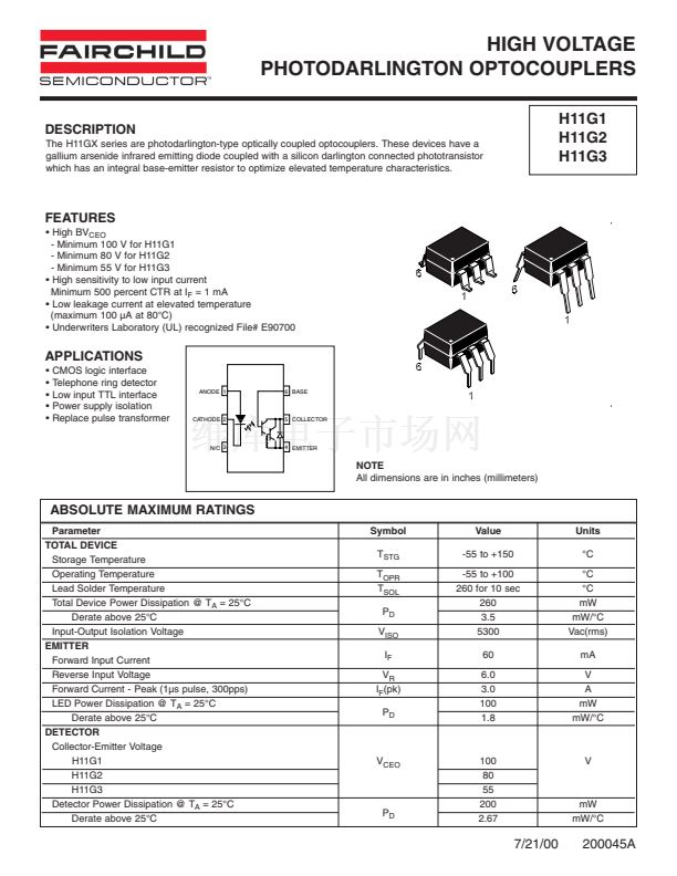
ANODE 1
6 BASE
CATHODE 2
5 COLLECTOR
N/C 3
4 EMITTER
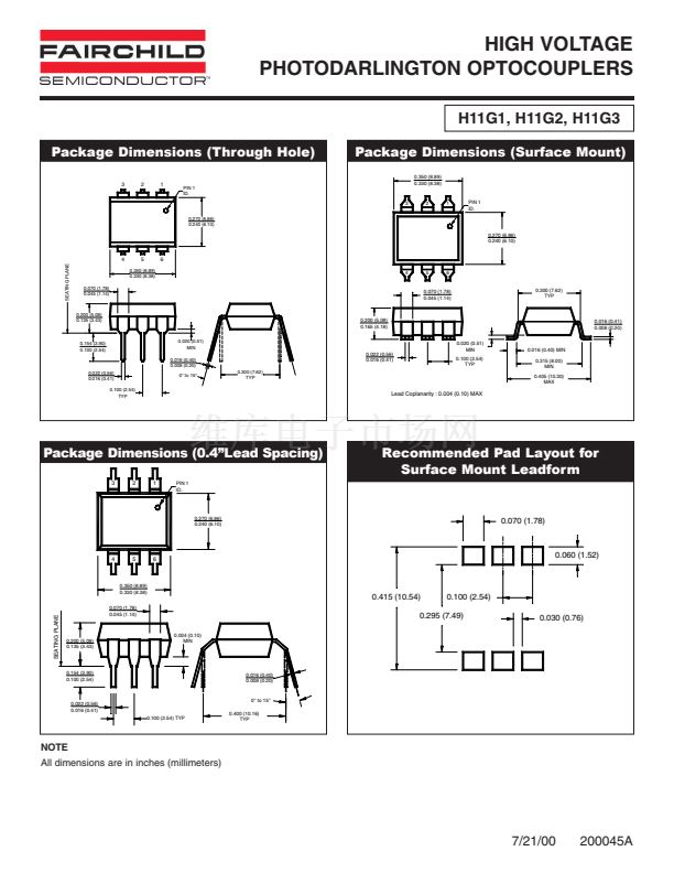
NOTE
All dimensions are in inches (millimeters)
ABSOLUTE MAXIMUM RATINGS
Parameter
TOTAL DEVICE
Storage Temperature
Operating Temperature
Lead Solder Temperature
Total Device Power Dissipation @ T
A
= 25掳C
Derate above 25掳C
Input-Output Isolation Voltage
EMITTER
Forward Input Current
Reverse Input Voltage
Forward Current - Peak (1碌s pulse, 300pps)
LED Power Dissipation @ T
A
= 25掳C
Derate above 25掳C
DETECTOR
Collector-Emitter Voltage
H11G1
H11G2
H11G3
Detector Power Dissipation @ T
A
= 25掳C
Derate above 25掳C
Symbol
T
STG
T
OPR
T
SOL
P
D
V
ISO
I
F
V
R
I
F
(pk)
P
D
Value
-55 to +150
-55 to +100
260 for 10 sec
260
3.5
5300
60
6.0
3.0
100
1.8
Units
掳C
掳C
掳C
mW
mW/掳C
Vac(rms)
mA
V
A
mW
mW/掳C
V
CEO
P
D
100
80
55
200
2.67
V
mW
mW/掳C
7/21/00
200045A


 1
1
 2
2
 3
3
 4
4
 5
5
 6
6
 7
7
