128K x 36, 256K x 18
3.3V Synchronous SRAMs
3.3V I/O, Pipelined Outputs
Burst Counter, Single Cycle Deselect
x
x
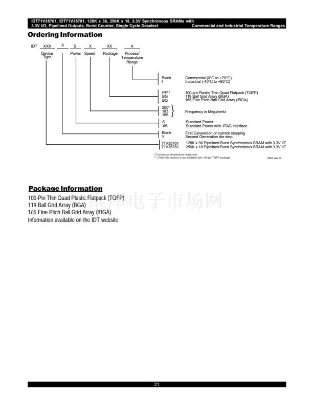
IDT71V35761S
IDT71V35781S
IDT71V35761SA
IDT71V35781SA
Features
128K x 36, 256K x 18 memory configurations
Supports high system speed:
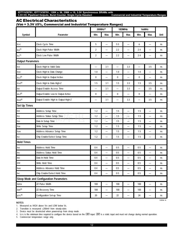
Commercial:
鈥?200MHz 3.1ns clock access time
Commercial and Industrial:
鈥?183MHz 3.3ns clock access time
鈥?166MHz 3.5ns clock access time
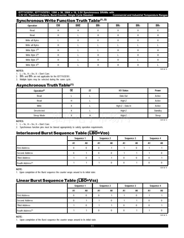
LBO
input selects interleaved or linear burst mode
Self-timed write cycle with global write control (GW), byte write
enable (BWE), and byte writes (BWx)
3.3V core power supply
Power down controlled by ZZ input
3.3V I/O
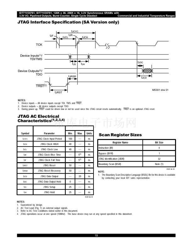
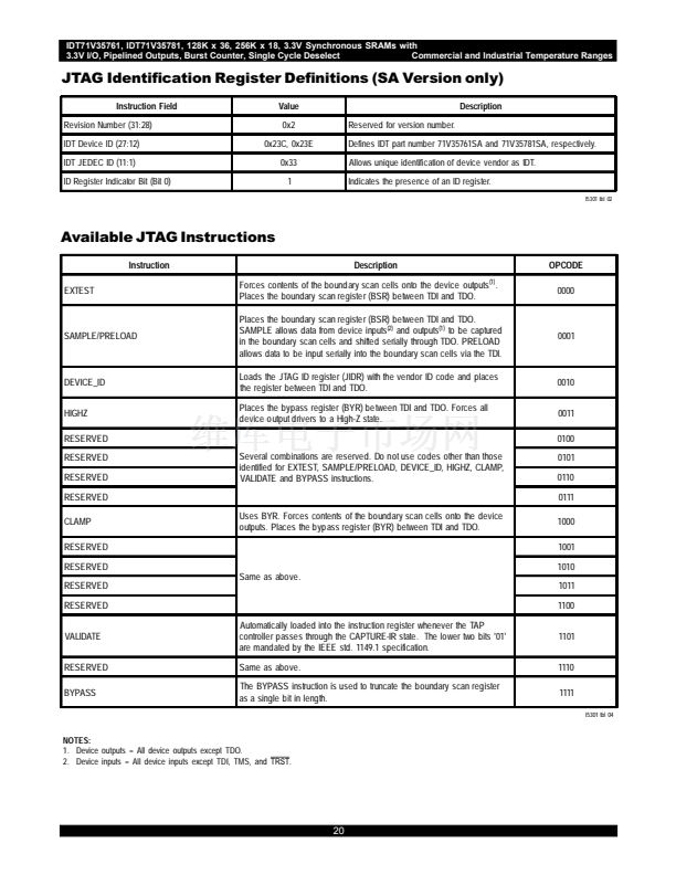
Optional - Boundary Scan JTAG Interface (IEEE 1149.1
compliant)
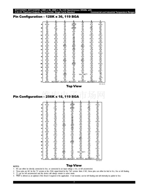
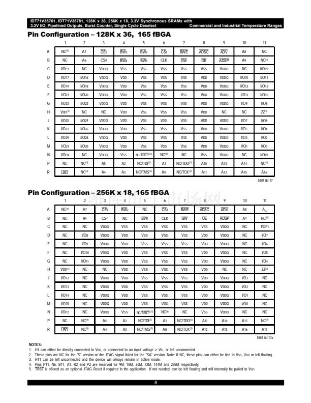
Packaged in a JEDEC Standard 100-pin plastic thin quad
flatpack (TQFP), 119 ball grid array (BGA) and 165 fine pitch ball
grid array
Description
The IDT71V35761/781 are high-speed SRAMs organized as
128K x 36/256K x 18. The IDT71V35761/781 SRAMs contain write, data,
address and control registers. Internal logic allows the SRAM to generate
a self-timed write based upon a decision which can be left until the end of
the write cycle.
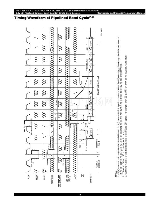
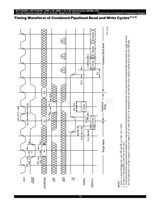
The burst mode feature offers the highest level of performance to the
system designer, as the IDT71V35761/81 can provide four cycles of data
for a single address presented to the SRAM. An internal burst address
counter accepts the first cycle address from the processor, initiating the
access sequence. The first cycle of output data will be pipelined for one
cycle before it is available on the next rising clock edge. If burst mode
operation is selected (ADV=LOW), the subsequent three cycles of output
data will be available to the user on the next three rising clock edges. The
order of these three addresses are defined by the internal burst counter
and the
LBO
input pin.
The IDT71V35761/781 SRAMs utilize IDT鈥檚 latest high-performance
CMOS process and are packaged in a JEDEC standard 14mm x 20mm
100-pin thin plastic quad flatpack (TQFP) as well as a 119 ball grid array
(BGA) and 165 fine pitch ball grid array.
Input
Input
Input
Input
Input
Input
Input
Input
Input
Input
Input
Input
Input
Input
Input
Output
Input
Input
I/O
Supply
Supply
Synchronous
Synchronous
Synchronous
Asynchronous
Synchronous
Synchronous
Synchronous
N/A
Synchronous
Synchronous
Synchronous
DC
Synchronous
Synchronous
N/A
Synchronous
Asynchronous
Asynchronous
Synchronous
N/A
N/A
5301 tbl 01
x
x
x
x
x
x
x
Pin Description Summary
A
0
-A
17
CE
CS
0
,
CS
1
OE
GW
BWE
BW
1
,
BW
2
,
BW
3
,
BW
4
(1)
CLK
ADV
ADSC
ADSP
LBO
TMS
TDI
TCK
TDO
TRST
ZZ
I/O
0
-I/O
31
, I/O
P1
-I/O
P4
V
DD
, V
DDQ
Address Inputs
Chip Enable
Chip Selects
Output Enable
Global Write Enable
Byte Write Enable
Individual Byte Write Selects
Clock
Burst Address Advance
Address Status (Cache Controller)
Address Status (Processor)
Linear / Interleaved Burst Order
Test Mode Select
Test Data Input
Test Clock
Test Data Output
JTAG Reset (Optional)
Sleep Mode
Data Input / Output
Core Power, I/O Power
V
SS
Ground
NOTE:
1.
BW
3
and
BW
4
are not applicable for the IDT71V35781.
1
漏2003 Integrated Device Technology, Inc.
JUNE 2003
DSC-5301/03


 1
1
 2
2
 3
3
 4
4
 5
5
 6
6
 7
7
 8
8
 9
9
 10
10
 11
11
 12
12
 13
13
 14
14
 15
15
 16
16
 17
17
 18
18
 19
19
 20
20
 21
21
 22
22
