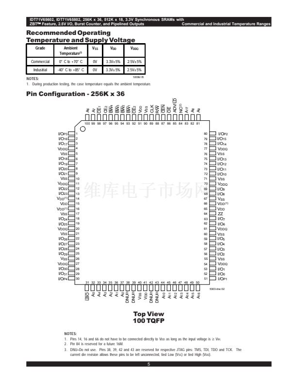
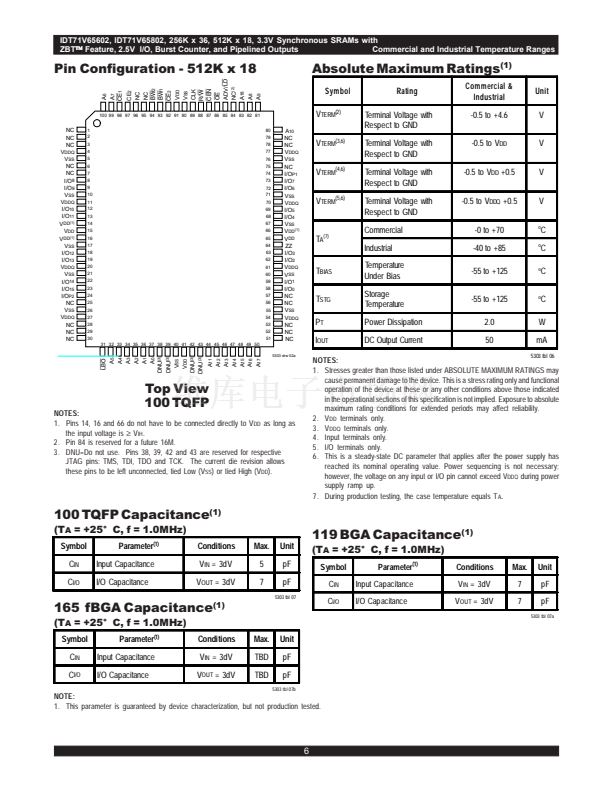
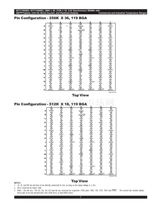
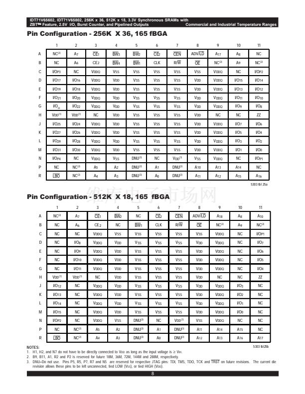
256K x 36, 512K x 18
3.3V Synchronous ZBT鈩?SRAMs
2.5V I/O, Burst Counter
Pipelined Outputs
x
x
x
x
x
x
x
x
x
x
x
x
x
IDT71V65602
IDT71V65802
Features
256K x 36, 512K x 18 memory configurations
Supports high performance system speed - 150MHz
(3.8ns Clock-to-Data Access)
ZBT
TM
Feature - No dead cycles between write and read cycles
Internally synchronized output buffer enable eliminates the
need to control
OE
Single R/W (READ/WRITE) control pin
W
Positive clock-edge triggered address, data, and control
signal registers for fully pipelined applications
4-word burst capability (interleaved or linear)
Individual byte write (BW
1
-
BW
4
) control (May tie active)
BW
Three chip enables for simple depth expansion
3.3V power supply (卤5%)
2.5V I/O Supply (V
DDQ
)
Power down controlled by ZZ input
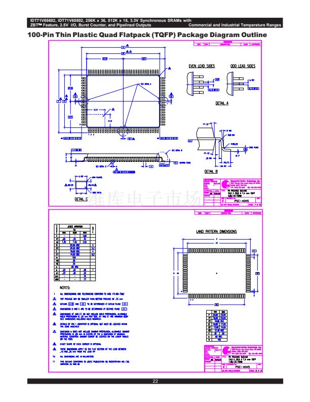
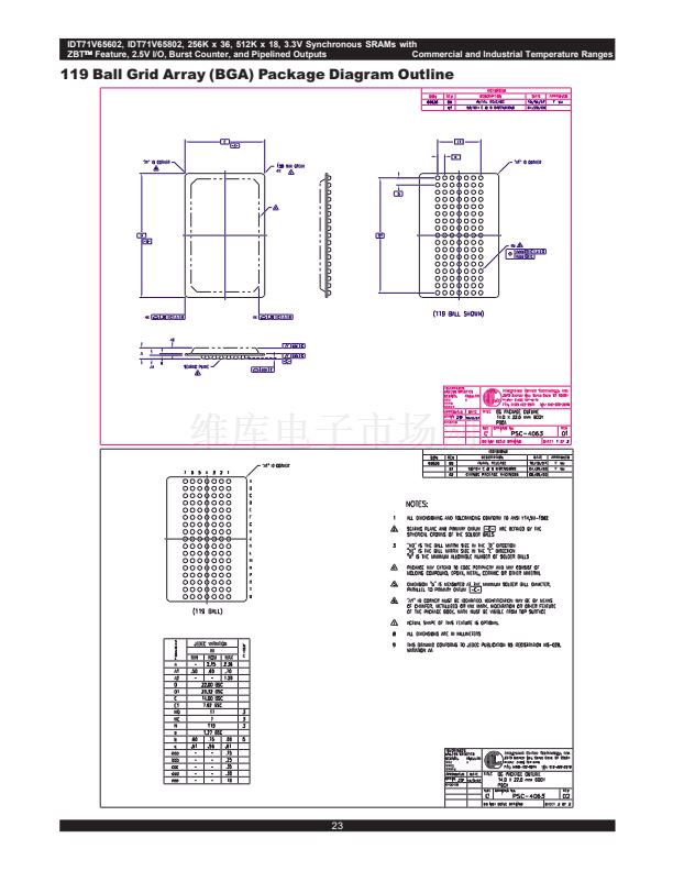
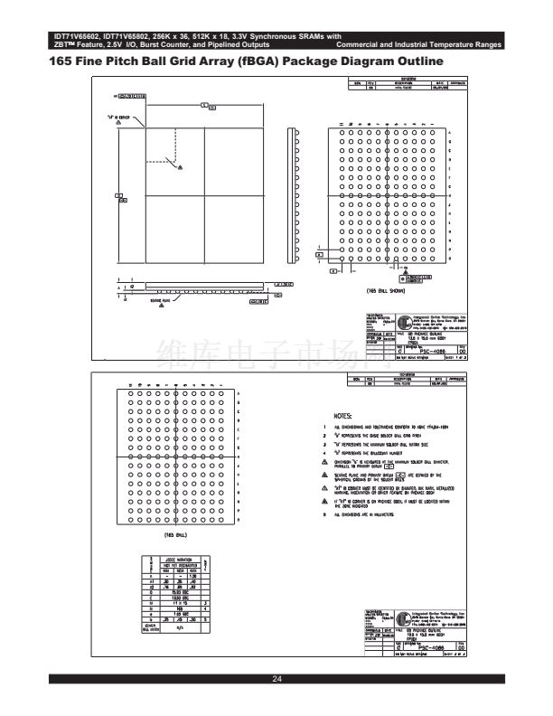
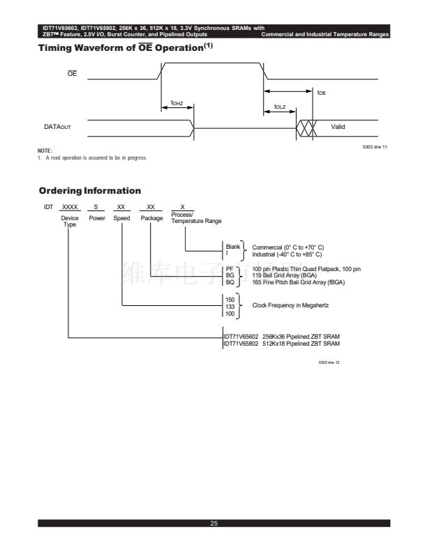
Packaged in a JEDEC standard 100-pin plastic thin quad and
flatpack (TQFP), 119 ball grid array (BGA) and 165 fine pitch
ball grid array (fBGA)
Description
The IDT71V65602/5802 are 3.3V high-speed 9,437,184-bit
(9 Megabit) synchronous SRAMs. They are designed to eliminate dead
bus cycles when turning the bus around between reads and writes, or
writes and reads. Thus, they have been given the name ZBT
TM
, or Zero
Bus Turnaround.
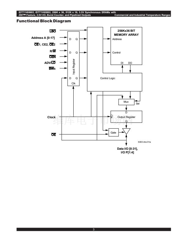
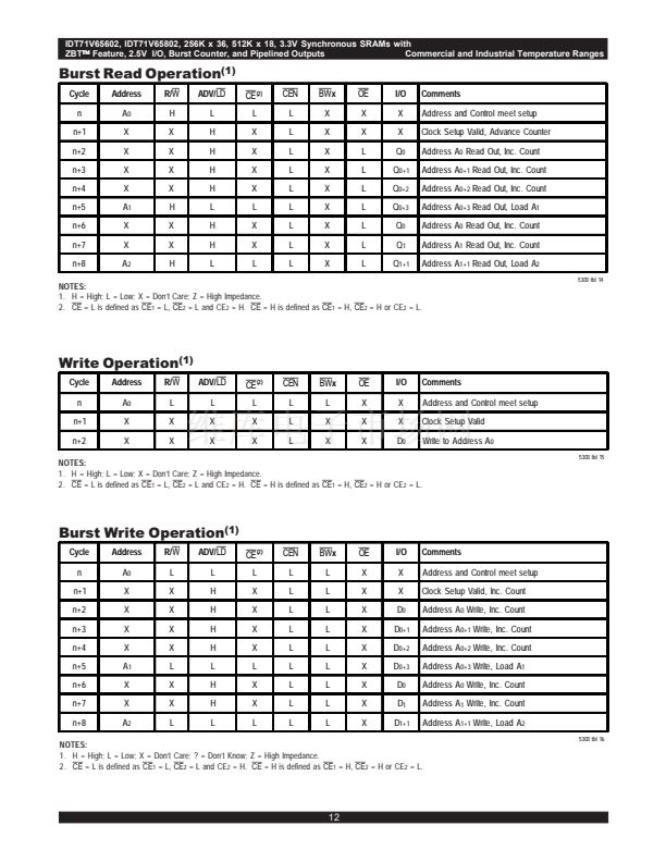
Address and control signals are applied to the SRAM during one clock
cycle, and two cycles later the associated data cycle occurs, be it read or write.
The IDT71V65602/5802 contain data I/O, address and control signal
registers. Output enable is the only asynchronous signal and can be used to
disable the outputs at any given time.
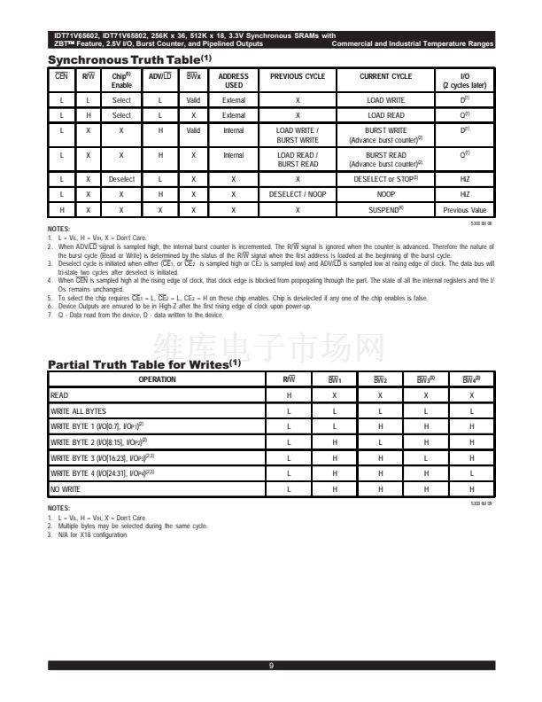
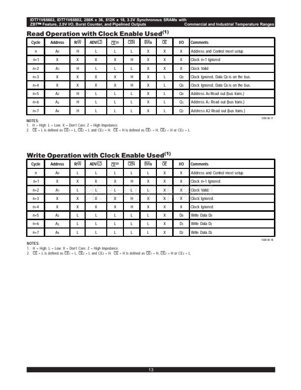
A Clock Enable (CEN) pin allows operation of the IDT71V65602/5802
to be suspended as long as necessary. All synchronous inputs are ignored
when (CEN) is high and the internal device registers will hold their previous
values.
There are three chip enable pins (CE
1
, CE
2
,
CE
2
) that allow the
user to deselect the device when desired. If any one of these three are not
asserted when ADV/LD is low, no new memory operation can be initiated.
However, any pending data transfers (reads or writes) will be completed. The
data bus will tri-state two cycles after chip is deselected or a write is initiated.
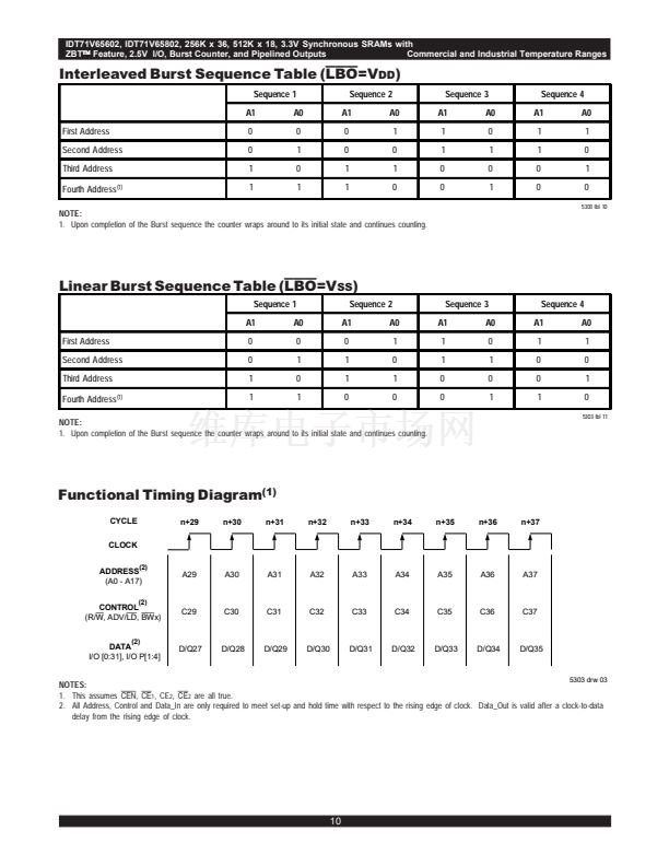
The IDT71V65602/5802 have an on-chip burst counter. In the burst
mode, the IDT71V65602/5802 can provide four cycles of data for a single
address presented to the SRAM. The order of the burst sequence is defined
by the
LBO
input pin. The
LBO
pin selects between linear and interleaved burst
sequence. The ADV/LD signal is used to load a new external address (ADV/
LD
= LOW) or increment the internal burst counter (ADV/LD = HIGH).
The IDT71V65602/5802 SRAM utilize IDT's latest high-performance
CMOS process, and are packaged in a JEDEC Standard 14mm x 20mm 100-
pin thin plastic quad flatpack (TQFP) as well as a 119 ball grid array (BGA)
and a 165 fine pitch ball grid array (fBGA).
Pin Description Summary
A
0
-A
18
Address Inputs
Chip Enables
Output Enable
Read/Write Signal
Clock Enable
Individual Byte Write Selects
Clock
Advance burst address / Load new address
Linear / Interleaved Burst Order
Sleep Mode
Data Input / Output
Core Power, I/O Power
Ground
Input
Input
Input
Input
Input
Input
Input
Input
Input
Input
I/O
Supply
Supply
Synchronous
Synchronous
Asynchronous
Synchronous
Synchronous
Synchronous
N/A
Synchronous
Static
Asynchronous
Synchronous
Static
Static
5303 tbl 01
CE
1
, CE
2
,
CE
2
OE
R/
W
CEN
BW
1
,
BW
2
,
BW
3
,
BW
4
CLK
ADV/
LD
LBO
ZZ
I/O
0
-I/O
31
, I/O
P1
-I/O
P4
V
DD
, V
DDQ
V
SS
ZBT and Zero Bus Turnaround are trademarks of Integrated Device Technology, Inc. and the architecture is supported by Micron Technology and Motorola, Inc.
OCTOBER 2004
DSC-5303/05
1
漏2004 Integrated Device Technology, Inc.


 1
1
 2
2
 3
3
 4
4
 5
5
 6
6
 7
7
 8
8
 9
9
 10
10
 11
11
 12
12
 13
13
 14
14
 15
15
 16
16
 17
17
 18
18
 19
19
 20
20
 21
21
 22
22
 23
23
 24
24
 25
25
 26
26
