鈥?/div>
0.5 MICRON CMOS Technology
ESD > 2000V per MIL-STD-883, Method 3015;
> 200V using machine model (C = 200pF, R = 0)
V
CC
= 3.3V 卤 0.3V, Normal Range
V
CC
= 2.7V to 3.6V, Extended Range
V
CC
= 2.5V 卤 0.2V
CMOS power levels (0.4碌 W typ. static)
Rail-to-Rail output swing for increased noise margin
Available in SOIC, SSOP and TSSOP packages
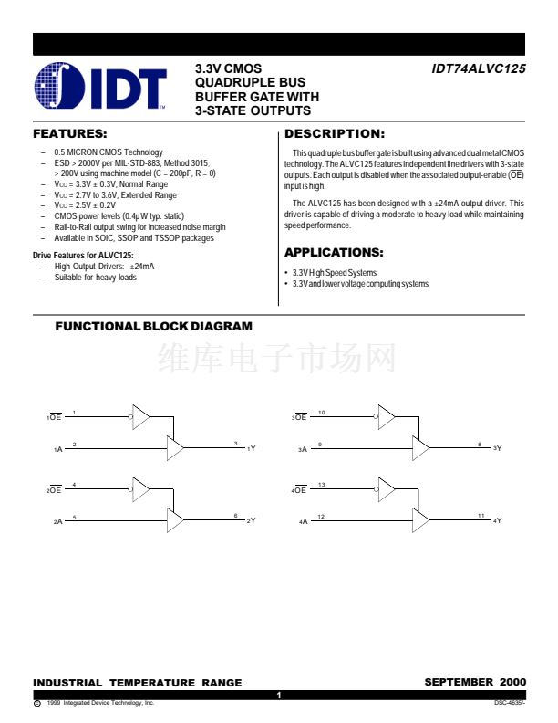
IDT74ALVC125
DESCRIPTION:
This quadruple bus buffer gate is built using advanced dual metal CMOS
technology. The ALVC125 features independent line drivers with 3-state
outputs. Each output is disabled when the associated output-enable (OE)
input is high.
The ALVC125 has been designed with a 卤24mA output driver. This
driver is capable of driving a moderate to heavy load while maintaining
speed performance.
Drive Features for ALVC125:
鈥?High Output Drivers: 卤24mA
鈥?Suitable for heavy loads
APPLICATIONS:
鈥?/div>
3.3V High Speed Systems
鈥?/div>
3.3V and lower voltage computing systems
FUNCTIONAL BLOCK DIAGRAM
1
OE
1
3
OE
10
1
A
2
3
1
Y
3
A
9
8
3
Y
2
OE
4
4
OE
13
2
A
5
6
2
Y
4
A
12
11
4
Y
INDUSTRIAL TEMPERATURE RANGE
1
c
1999 Integrated Device Technology, Inc.
SEPTEMBER 2000
DSC-4635/-


 1
1
 2
2
 3
3
 4
4
 5
5
 6
6
