鈥?/div>
Typical
t
SK(0)
(Output Skew) < 250ps
ESD > 2000V per MIL-STD-883, Method 3015;
> 200V using machine model (C = 200pF, R = 0)
0.635mm pitch SSOP, 0.50mm pitch TSSOP
and 0.40mm pitch TVSOP packages
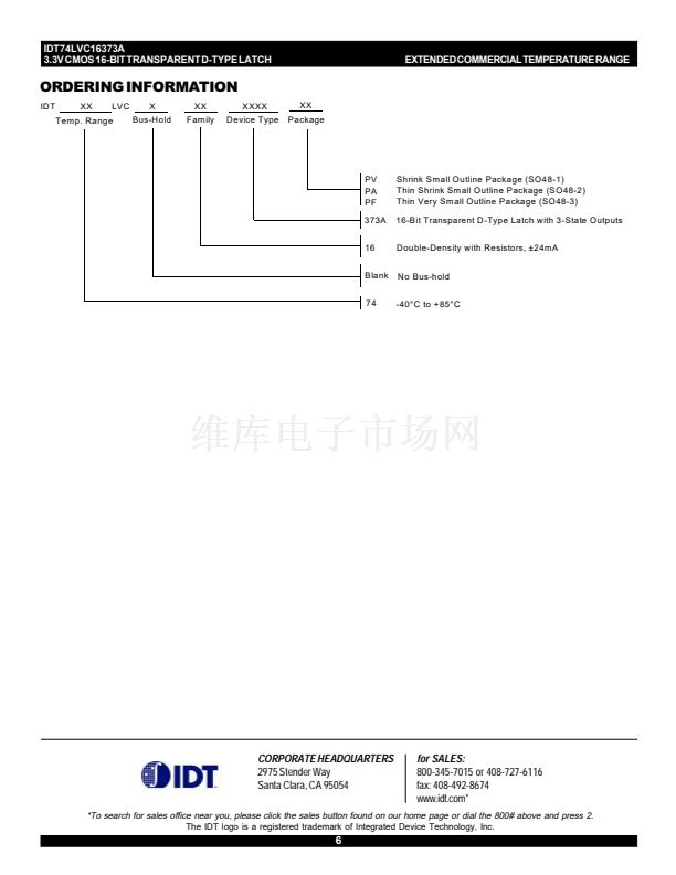
Extended commercial range of -40掳C to +85掳C
V
CC
= 3.3V 卤0.3V, Normal Range
V
CC
= 2.7V to 3.6V, Extended Range
CMOS power levels (0.4碌 W typ. static)
All inputs, outputs and I/O are 5 Volt tolerant
Supports hot insertion
IDT74LVC16373A
DESCRIPTION:
The LVC16373A 16-bit transparent D-type latch is built using advanced
dual metal CMOS technology. This high-speed, low-power latch is ideal
for temporary storage of data. The LVC16373A can be used for implement-
ing memory address latches, I/O ports, and bus drivers. The Output Enable
and Latch Enable controls are organized to operate each device as two 8-
bit latches or one 16-bit latch. Flow-through organization of signal pins
simplifies layout. All inputs are designed with hysteresis for improved noise
margin.
All pins of the LVC16373A can be driven from either 3.3V or 5V devices.
This feature allows the use of this device as a translator in a mixed 3.3V/
5V supply system.
The LVC16373A has been designed with a
卤
24mA output driver. This
driver is capable of driving a moderate to heavy load while maintaining
speed performance.
Drive Features for LVC16373A:
鈥?High Output Drivers: 卤24mA
鈥?Reduced system switching noise
APPLICATIONS:
鈥?5V and 3.3V mixed voltage systems
鈥?Data communication and telecommunication systems
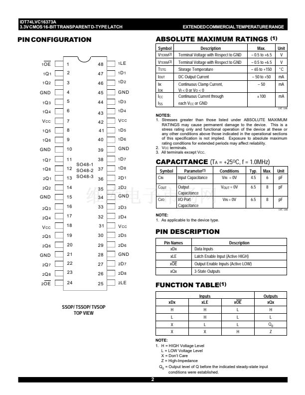
Functional Block Diagram
1
OE
1
2
OE
24
1
LE
48
2
LE
25
1
D
1
47
D
2
2
D
1
36
D
13
C Q
1
Q
1
C Q
2
Q
1
TO SEVEN OTHER CHANNELS
TO SEVEN OTHER CHANNELS
EXTENDED COMMERCIAL TEMPERATURE RANGE
1
c
1999 Integrated Device Technology, Inc.
MARCH 1999
DSC-4624/1


 1
1
 2
2
 3
3
 4
4
 5
5
 6
6
