鈥?/div>
160-MHz clock support
LVPECL or LVCMOS/LVTTL clock input
LVCMOS/LVTTL compatible inputs
12 clock outputs: drive up to 24 clock lines
Synchronous Output Enable
Output three-state control
350-ps maximum output-to-output skew
Pin compatible with MPC948
Industrial temp. range: 鈥?0掳C to +85掳C
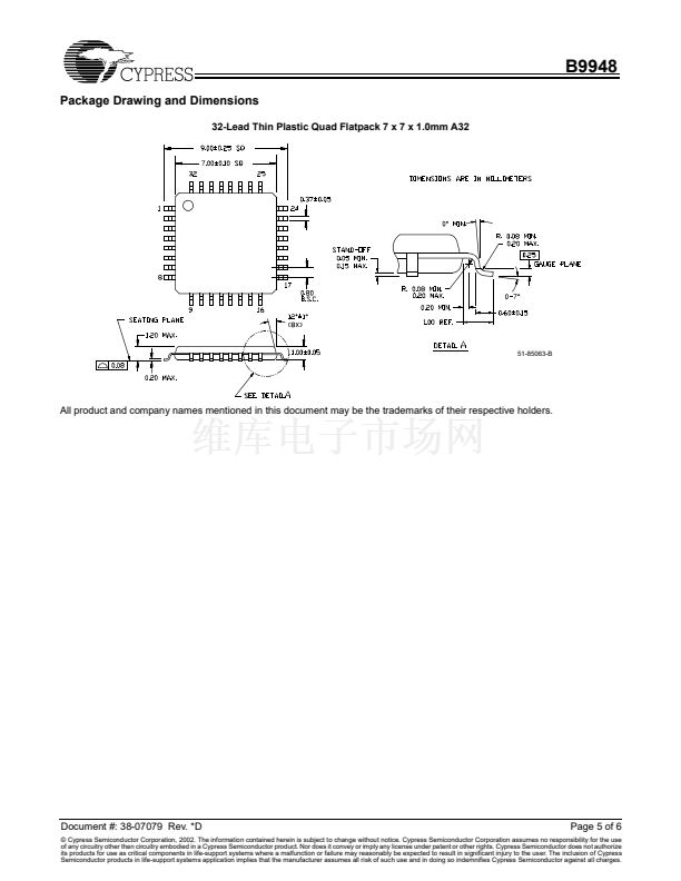
32-pin TQFP package
Description
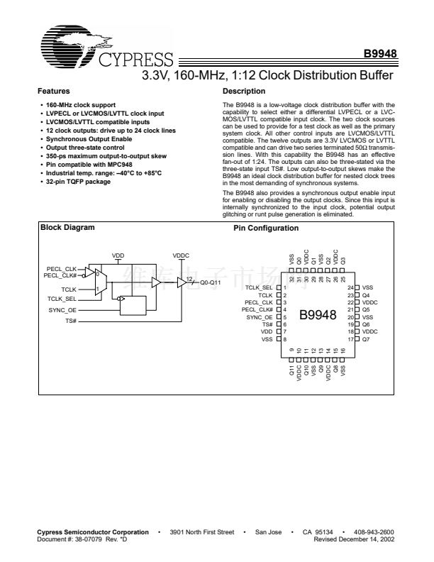
The B9948 is a low-voltage clock distribution buffer with the
capability to select either a differential LVPECL or a LVC-
MOS/LVTTL compatible input clock. The two clock sources
can be used to provide for a test clock as well as the primary
system clock. All other control inputs are LVCMOS/LVTTL
compatible. The twelve outputs are 3.3V LVCMOS or LVTTL
compatible and can drive two series terminated 50鈩?transmis-
sion lines. With this capability the B9948 has an effective
fan-out of 1:24. The outputs can also be three-stated via the
three-state input TS#. Low output-to-output skews make the
B9948 an ideal clock distribution buffer for nested clock trees
in the most demanding of synchronous systems.
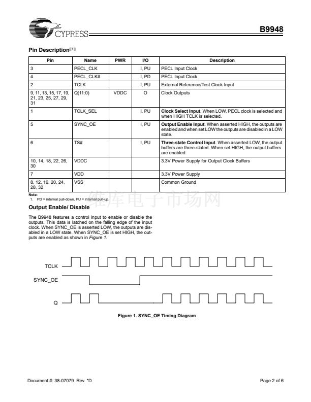
The B9948 also provides a synchronous output enable input
for enabling or disabling the output clocks. Since this input is
internally synchronized to the input clock, potential output
glitching or runt pulse generation is eliminated.
Block Diagram
Pin Configuration
VSS
Q0
VDDC
Q1
VSS
Q2
VDDC
Q3
VDD
PECL_CLK
PECL_CLK#
TCLK
TCLK_SEL
SYNC_OE
TS#
0
1
VDDC
12
Q0-Q11
TCLK_SEL
TCLK
PECL_CLK
PECL_CLK#
SYNC_OE
TS#
VDD
VSS
1
2
3
4
5
6
7
8
32
31
30
29
28
27
26
25
24
23
22
21
20
19
18
17
B9948
9
10
11
12
13
14
15
16
VSS
Q4
VDDC
Q5
VSS
Q6
VDDC
Q7
Cypress Semiconductor Corporation
Document #: 38-07079 Rev. *D
鈥?/div>
3901 North First Street
鈥?/div>
San Jose
Q11
VDDC
Q10
VSS
Q9
VDDC
Q8
VSS
鈥?/div>
CA 95134 鈥?408-943-2600
Revised December 14, 2002


 1
1
 2
2
 3
3
 4
4
 5
5
 6
6
