鈥?/div>
CMOS low power operation:
鈥?135 mW (typical) operating
鈥?16.5 碌W (typical) standby
鈥?Low data retention voltage: 2V (min.)
鈥?Output Enable (OE) and Chip Enable
(CE) inputs for ease in applications
鈥?TTL compatible inputs and outputs
鈥?Fully static operation:
鈥?No clock or refresh required
鈥?Single 2.7V (min) to 3.15V (max) V
CC
power supply
鈥?Available in 36-pin mini BGA
ISSI
DESCRIPTION
庐
MAY 2001
The
ISSI
IS62LV5128LL is a low voltage, 524,288 words by
8 bits, CMOS SRAM. It is fabricated using
ISSI
鈥?/div>
s low voltage,
six transistor (6T), CMOS technology. The device is targeted to
satisfy the demands of the state-of-the-art technologies
such as cell phones and pagers.
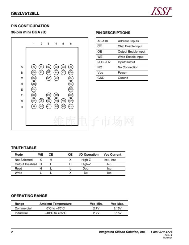
When
CE
is HIGH (deselected), the device assumes a
standby mode at which the power dissipation can be reduced
down with CMOS input levels. Additionally, easy memory
expansion is provided by using Chip Enable and Output
Enable inputs,
CE
and
OE.
The active LOW Write Enable (WE)
controls both writing and reading of the memory.
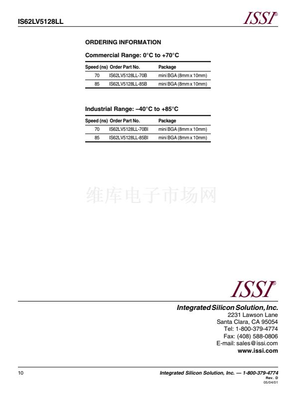
The IS62LV5128LL is available in a 36-pin mini BGA
package (8mm x 10mm).
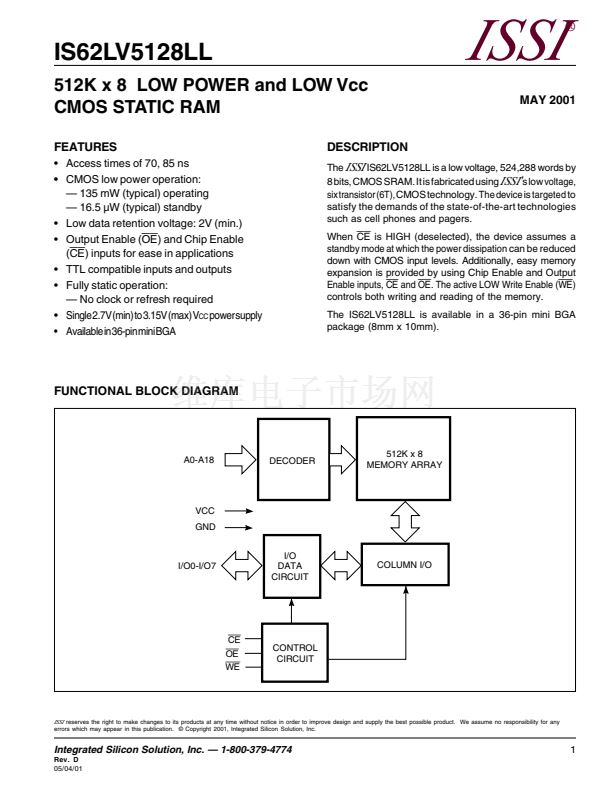
FUNCTIONAL BLOCK DIAGRAM
A0-A18
DECODER
512K x 8
MEMORY ARRAY
VCC
GND
I/O
DATA
CIRCUIT
I/O0-I/O7
COLUMN I/O
CE
OE
WE
CONTROL
CIRCUIT
ISSI
reserves the right to make changes to its products at any time without notice in order to improve design and supply the best possible product. We assume no responsibility for any
errors which may appear in this publication. 漏 Copyright 2001, Integrated Silicon Solution, Inc.
Integrated Silicon Solution, Inc. 鈥?1-800-379-4774
Rev. D
05/04/01
1


 1
1
 2
2
 3
3
 4
4
 5
5
 6
6
 7
7
 8
8
 9
9
 10
10
