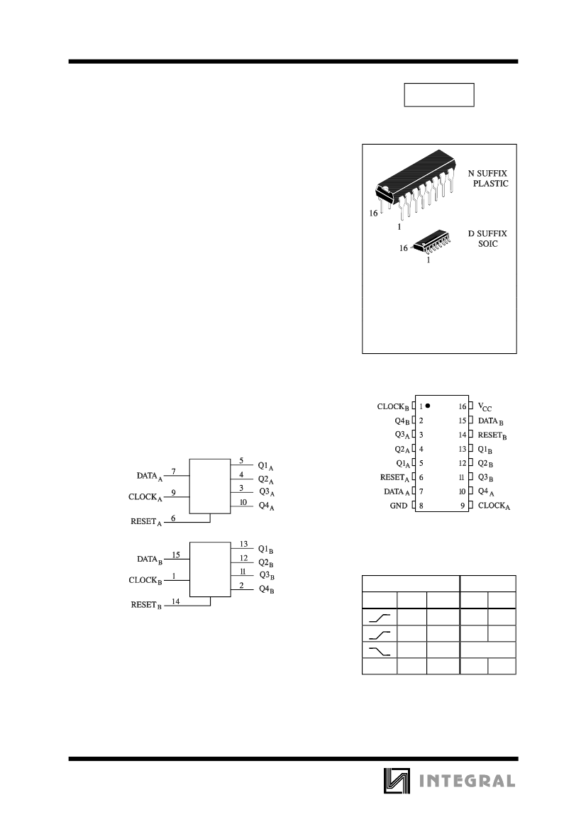
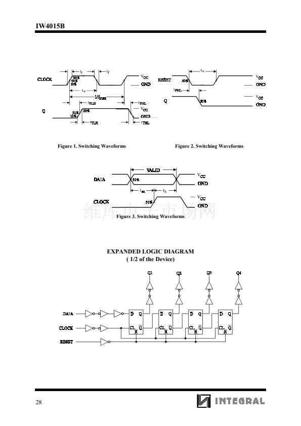
serial-input/parallel-output registers. Each register has independent
CLOCK and RESET inputs as well as a single serial DATA input. 鈥淨鈥?/div>
outputs are available from each of the four stages on both registers. All
register stages are D-type, master-slave flip-flops. The logic level
present at the DATA input is transferred into the first register stage and
shifted over one stage at each positive-going clock transition. Resetting
of all stages is accomplished by a high level on the reset line. Register
expansion to 8 stages using one IW4015B package, or to more than 8
stages using additional IW4015B鈥檚 is possible.
鈥?/div>
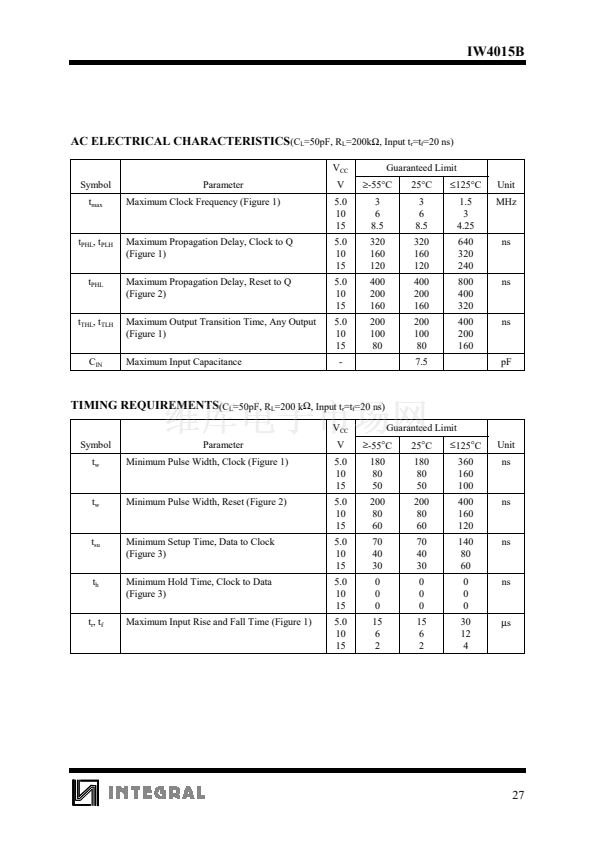
Operating Voltage Range: 3.0 to 18 V
鈥?/div>
Maximum input current of 1
碌A
at 18 V over full package-
temperature range; 100 nA at 18 V and 25掳C
鈥?/div>
Noise margin (over full package temperature range):
1.0 V min @ 5.0 V supply
2.0 V min @ 10.0 V supply
2.5 V min @ 15.0 V supply
ORDERING INFORMATION
IW4015BN Plastic
IW4015BD SOIC
T
A
= -55掳 to 125掳 C for all packages
PIN ASSIGNMENT
LOGIC DIAGRAM
FUNCTION TABLE
Inputs
Clock
Data
L
H
PIN 16=V
CC
PIN 8= GND
X
X
X
Reset
L
L
L
H
Outputs
Q1
L
H
L
Q
n
Q
n-1
Q
n-1
L
No change
X = don鈥檛 care
24


 1
1
 2
2
 3
3
 4
4
 5
5
