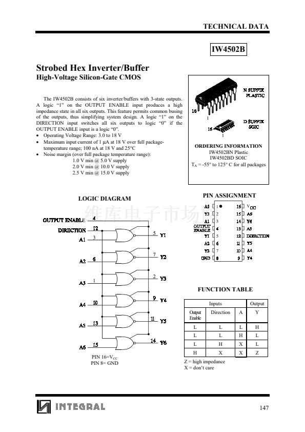
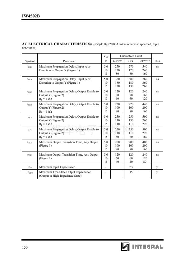
TECHNICAL DATA
IW4502B
Strobed Hex Inverter/Buffer
High-Voltage Silicon-Gate CMOS
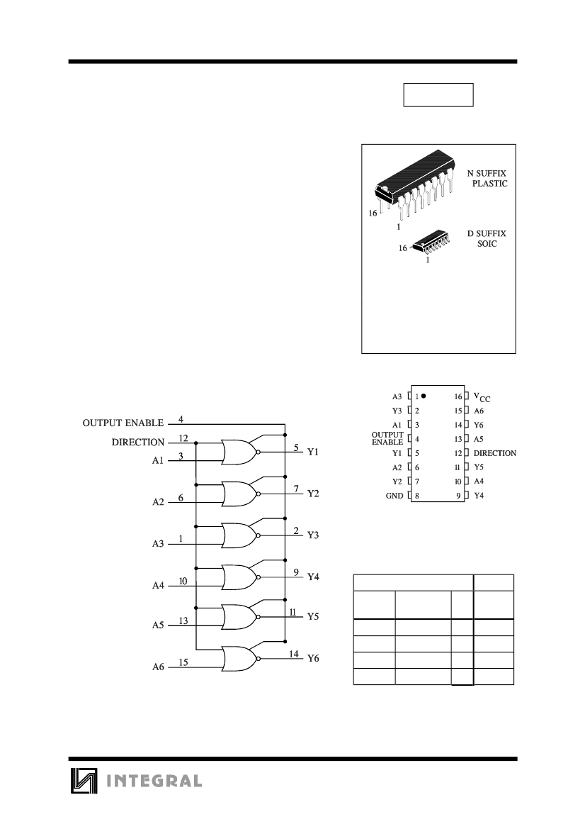
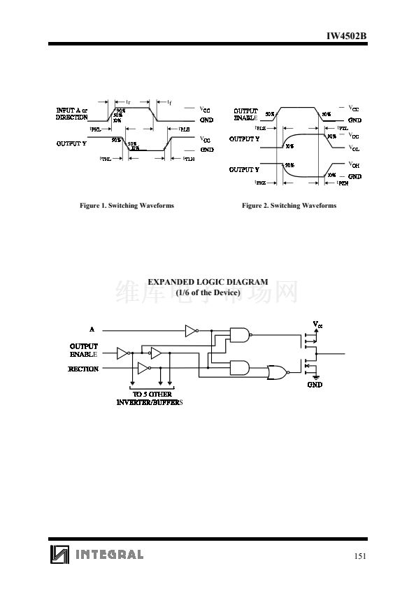
The IW4502B consists of six inverter/buffers with 3-state outputs.
A logic 鈥?鈥?on the OUTPUT ENABLE input produces a high
impedance state in all six outputs. This feature permits common busing
of the outputs, thus simplifying system design. A logic 鈥?鈥?on the
DIRECTION input switches all six outputs to logic 鈥?鈥?if the
OUTPUT ENABLE input is a logic 鈥?鈥?
鈥?/div>
Operating Voltage Range: 3.0 to 18 V
鈥?/div>
Maximum input current of 1
碌A
at 18 V over full package-
temperature range; 100 nA at 18 V and 25掳C
鈥?/div>
Noise margin (over full package temperature range):
1.0 V min @ 5.0 V supply
2.0 V min @ 10.0 V supply
2.5 V min @ 15.0 V supply
ORDERING INFORMATION
IW4502BN Plastic
IW4502BD SOIC
T
A
= -55掳 to 125掳 C for all packages
LOGIC DIAGRAM
PIN ASSIGNMENT
FUNCTION TABLE
Inputs
Output
Enable
L
L
L
PIN 16=V
CC
PIN 8= GND
H
Direction
L
L
H
X
A
L
H
X
X
Output
Y
H
L
L
Z
Z = high impedance
X = don鈥檛 care
147


 1
1
 2
2
 3
3
 4
4
 5
5
