LTC1555/LTC1556
SIM Power Supply
and Level Translator
FEATURES
s
s
s
DESCRIPTION
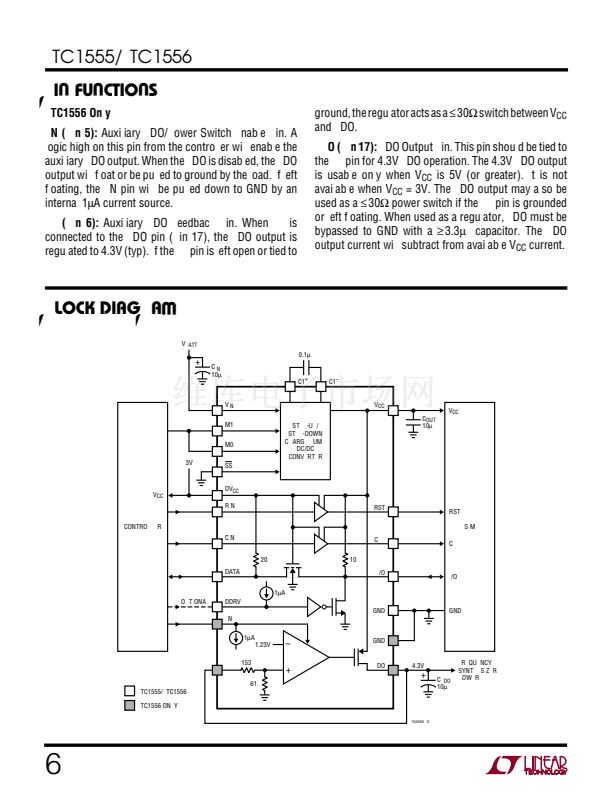
The LTC
庐
1555/LTC1556 provide power conversion and
level shifting needed for 3V GSM cellular telephones to
interface with either 3V or 5V Subscriber Identity Mod-
ules (SIMs). These parts contain a charge pump DC/DC
converter that delivers a regulated 5V to the SIM card.
Input voltage may range from 2.7V to 10V, allowing
direct connection to the battery. Output voltage may be
programmed to 3V, 5V or direct connection to the V
IN
pin.
A soft start feature limits inrush current at turn-on,
mitigating start-up problems that may result when the
input is supplied by another low power DC/DC converter.
The LTC1556 also includes an auxiliary LDO regulator/
power switch that may be used to power the frequency
synthesizer or other low power circuitry.
Battery life is maximized by 60碌A operating current and
1碌A shutdown current. Board area is minimized by minia-
ture 16- and 20-pin narrow SSOP packages and the need
for only three small external capacitors.
, LTC and LT are registered trademarks of Linear Technology Corporation.
s
s
s
s
s
s
s
s
s
s
Step-Up/Step-Down Charge Pump Generates 5V
Input Voltage Range: 2.7V to 10V
Output Current: 10mA (V
IN
鈮?/div>
2.7V)
20mA (V
IN
鈮?/div>
3V)
3V to 5V Signal Level Translators
> 10kV ESD on All SIM Contact Pins
Short-Circuit and Overtemperature Protected
Very Low Operating Current: 60碌A
Very Low Shutdown Current: < 1碌A
Soft Start Limits Inrush Current at Turn-On
Programmable 3V or 5V Output Voltage
650kHz Switching Frequency
Auxiliary 4.3V LDO/Power Switch (LTC1556 Only)
Available in a 16- and 20-Pin Narrow SSOP
APPLICATIONS
s
s
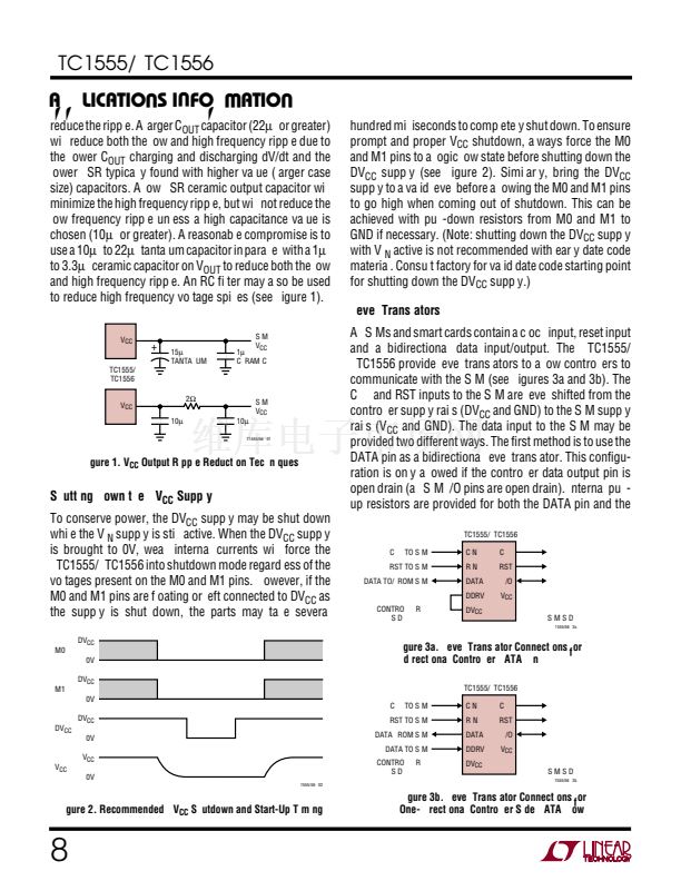
SIM Interface in GSM Cellular Telephones
Smart Card Readers
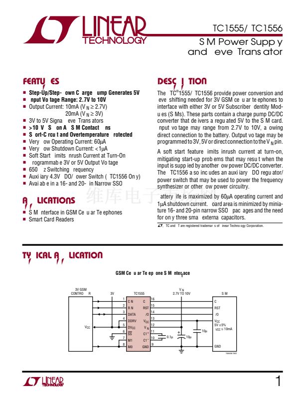
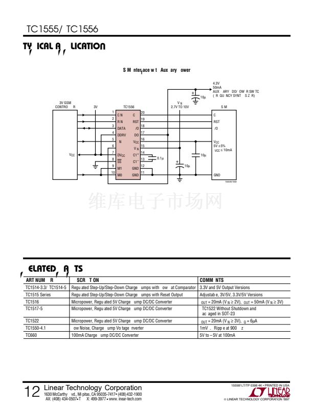
TYPICAL APPLICATION
GSM Cellular Telephone SIM Interface
3V GSM
CONTROLLER
3V
1
2
3
4
LTC1555
CIN
RIN
DATA
DDRV
DV
CC
SS
M1
M0
CLK
RST
I/O
V
CC
V
IN
C1
+
C1
鈥?/div>
GND
16
15
14
13
12
11
10
9
V
IN
2.7V TO 10V
CLK
RST
I/O
V
CC
5
6
7
8
+
0.1碌F
10碌F
U
U
U
SIM
10碌F
V
CC
5V
卤
5%
I
VCC
鈮?/div>
10mA
GND
1555/56 TA01
1


 1
1
 2
2
 3
3
 4
4
 5
5
 6
6
 7
7
 8
8
 9
9
 10
10
 11
11
 12
12
