M29F002BT, M29F002BNT
M29F002BB, M29F002BNB
2 Mbit (256Kb x8, Boot Block) Single Supply Flash Memory
s
SINGLE 5V 卤 10% SUPPLY VOLTAGE for
PROGRAM, ERASE and READ OPERATIONS
ACCESS TIME: 45 ns
PROGRAMMING TIME
鈥?8 碌s by Byte typical
7 MEMORY BLOCKS
鈥?1 Boot Block (Top or Bottom Location)
鈥?2 Parameter and 4 Main Blocks
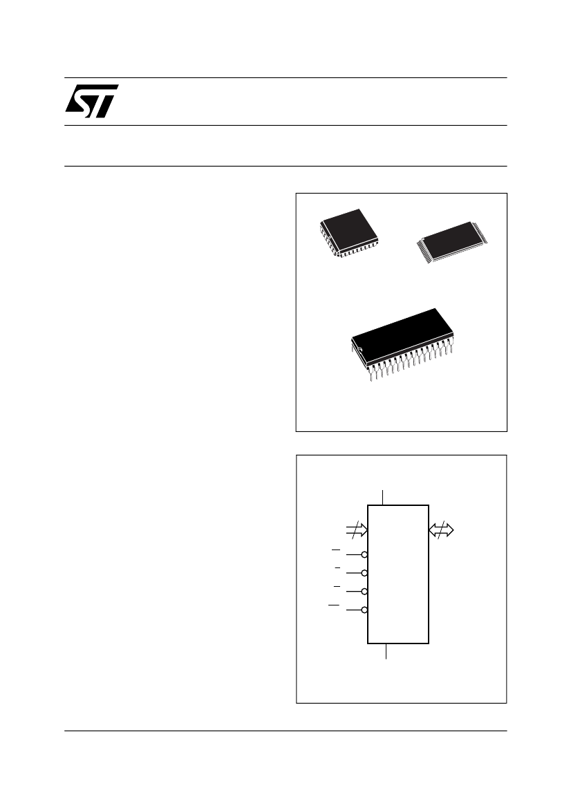
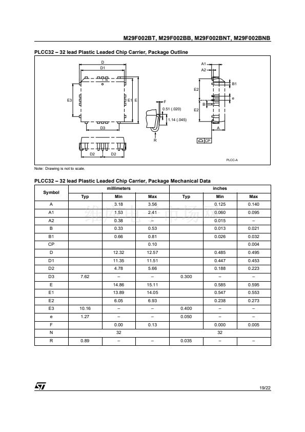
PLCC32 (K)
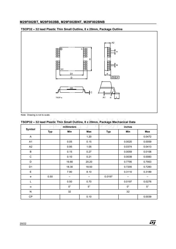
TSOP32 (N)
8 x 20mm
s
s
s
s
PROGRAM/ERASE CONTROLLER
鈥?Embedded Byte Program algorithm
鈥?Embedded Multi-Block/Chip Erase algorithm
鈥?Status Register Polling and Toggle Bits
32
s
ERASE SUSPEND and RESUME MODES
鈥?Read and Program another Block during
Erase Suspend
1
PDIP32 (P)
s
UNLOCK BYPASS PROGRAM COMMAND
鈥?Faster Production/Batch Programming
TEMPORARY BLOCK UNPROTECTION
MODE
LOW POWER CONSUMPTION
鈥?Standby and Automatic Standby
VCC
s
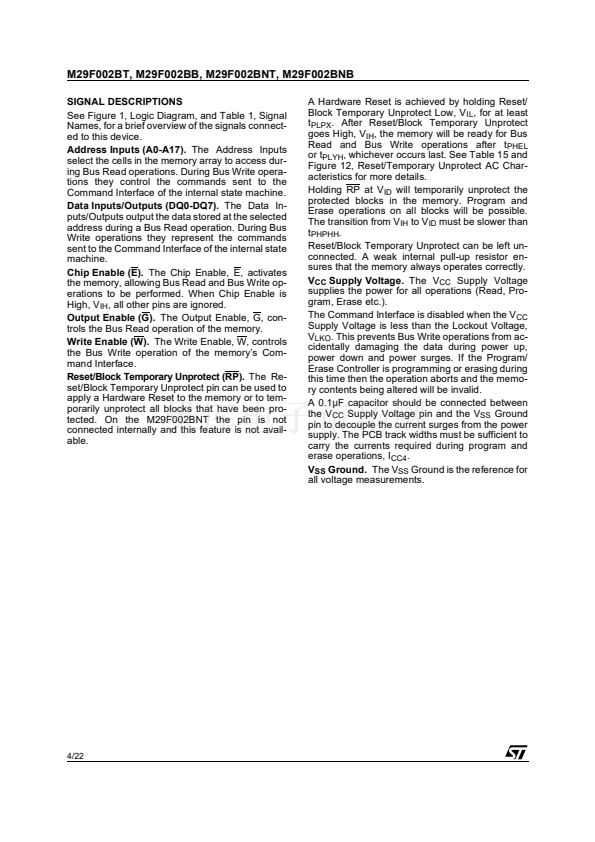
Figure 1. Logic Diagram
s
s
100,000 PROGRAM/ERASE CYCLES per
BLOCK
20 YEARS DATA RETENTION
鈥?Defectivity below 1 ppm/year
ELECTRONIC SIGNATURE
鈥?Manufacturer Code: 20h
鈥?Top Device Code M29F002BT: B0h
鈥?Top Device Code M29F002BNT: B0h
鈥?Bottom Device Code M29F002BB: 34h
鈥?Bottom Device Code M29F002BNB: 34h
G
RP
A0-A17
W
E
18
8
DQ0-DQ7
M29F002BT
M29F002BB
M29F002BNT
M29F002BNB
s
s
VSS
AI02957B
April 2002
1/22


 1
1
 2
2
 3
3
 4
4
 5
5
 6
6
 7
7
 8
8
 9
9
 10
10
 11
11
 12
12
 13
13
 14
14
 15
15
 16
16
 17
17
 18
18
 19
19
 20
20
 21
21
 22
22
