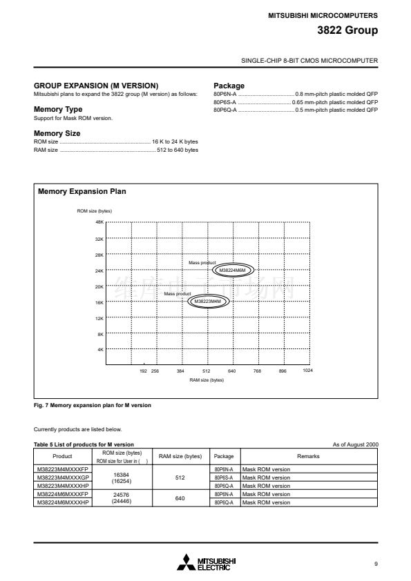
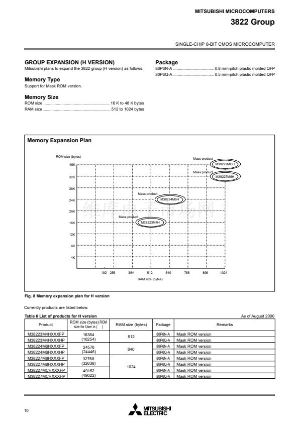
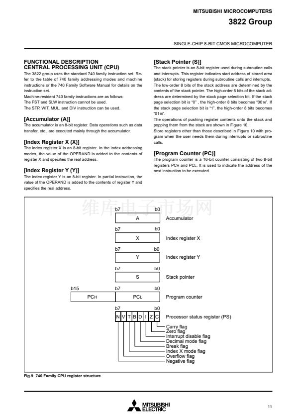
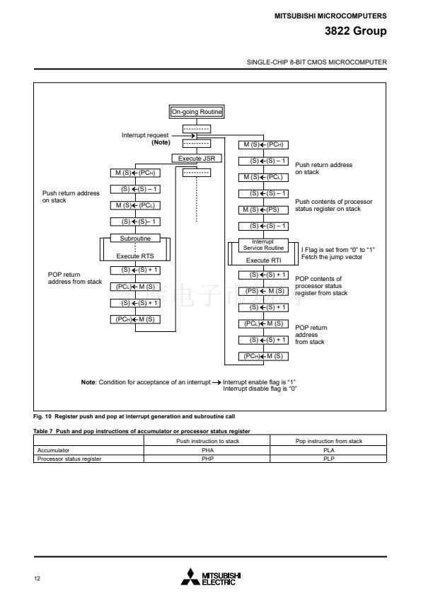
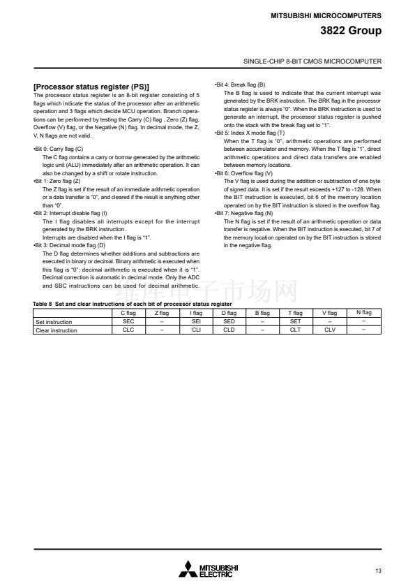
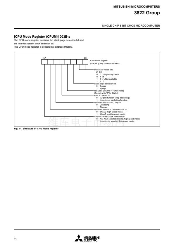
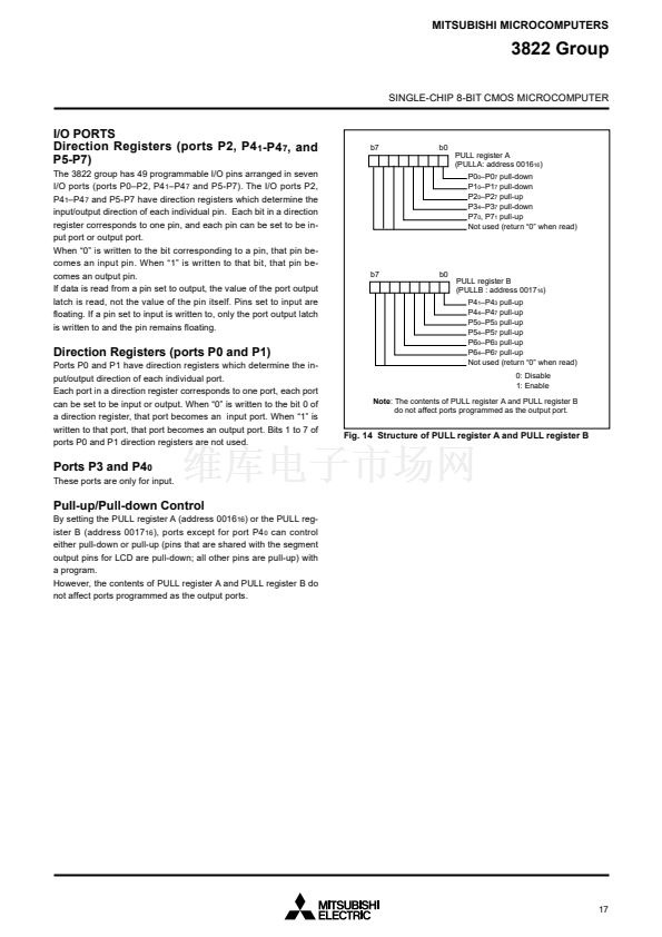
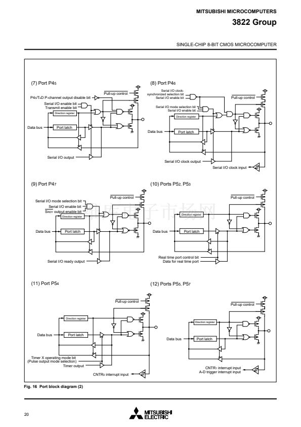
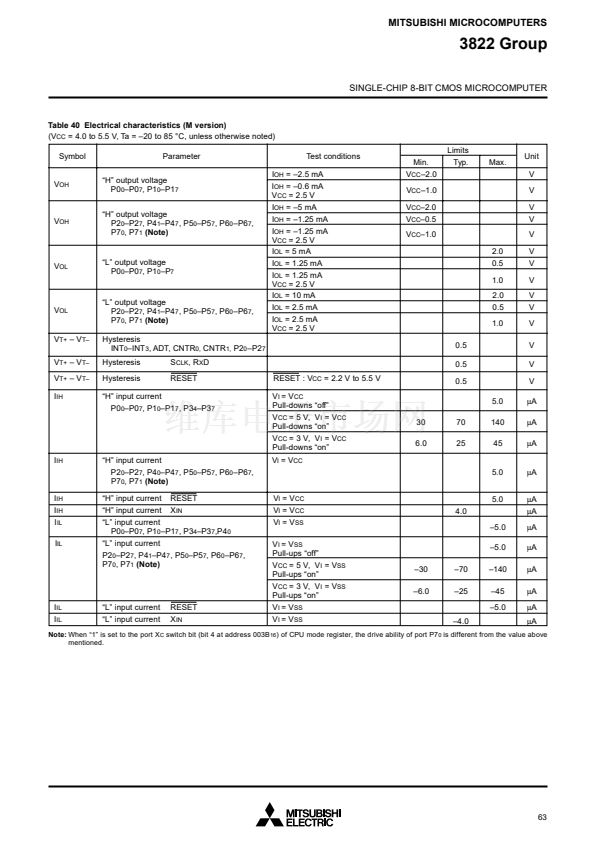
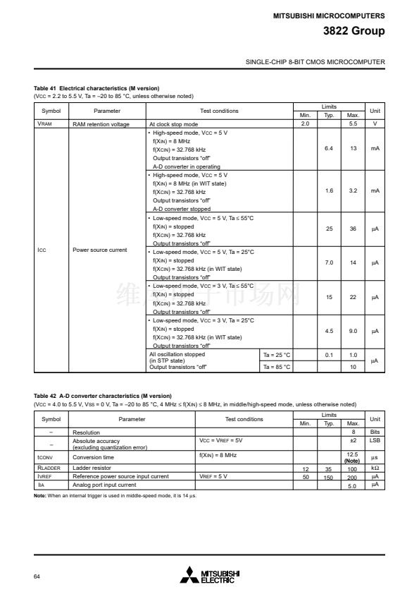
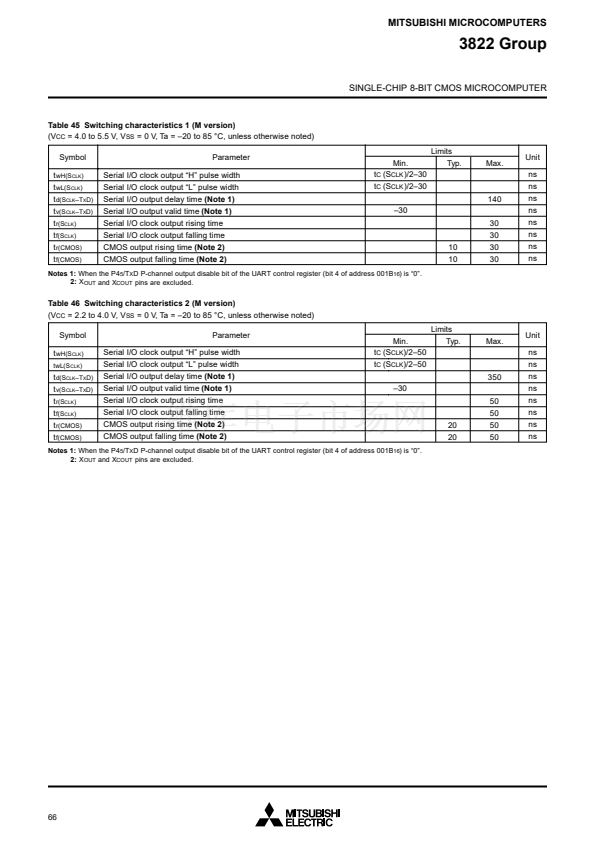
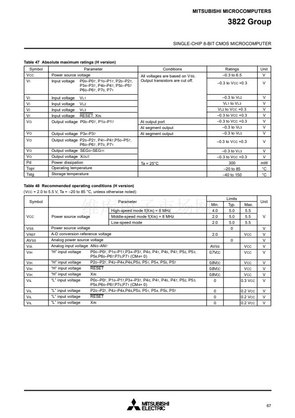
converter ................................................. 8-bit
鉁?/div>
8 channels
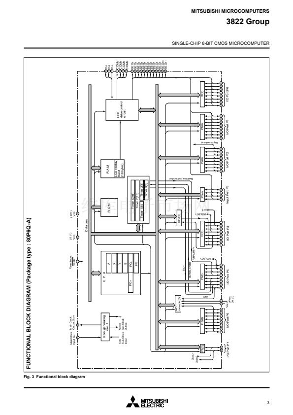
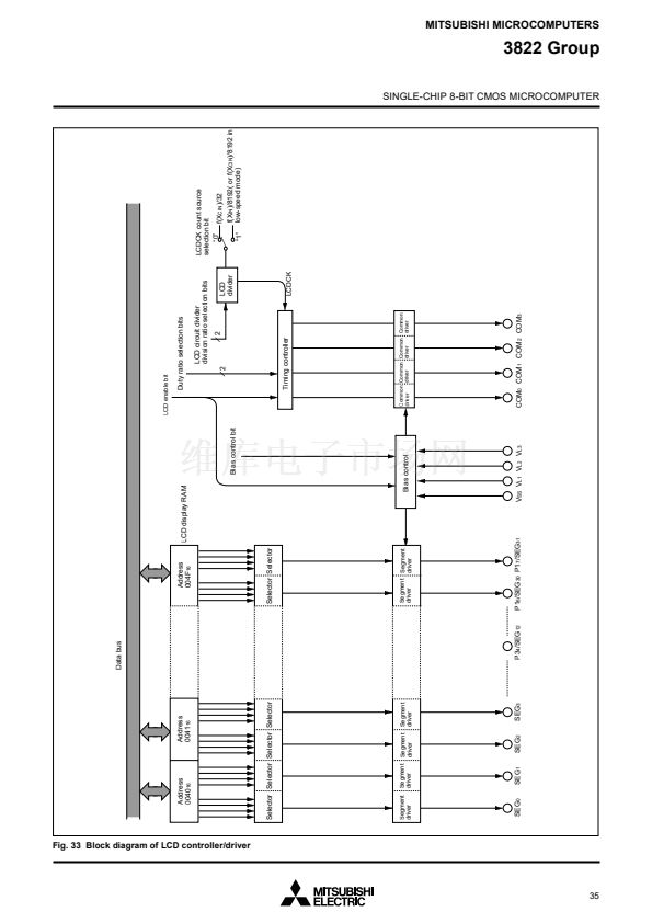
qLCD
drive control circuit
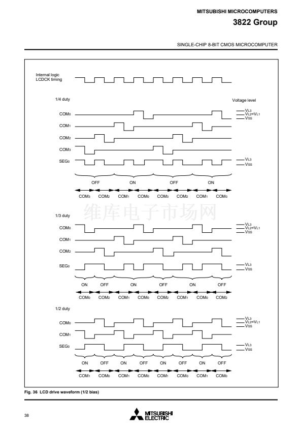
Bias ................................................................................... 1/2, 1/3
Duty ........................................................................... 1/2, 1/3, 1/4
Common output .......................................................................... 4
Segment output ........................................................................ 32
q2
clock generating circuits
(connect to external ceramic resonator or quartz-crystal oscillator)
qPower
source voltage
In high-speed mode .................................................. 4.0 to 5.5 V
In middle-speed mode ............................................... 2.5 to 5.5 V
(Extended operating temperature version:
2.0 to 5.5 V, Ta= 鈥?20 to 85掳C
3.0 to 5.5 V, Ta= 鈥?40 to 鈥?20掳C)
(One time PROM version: 2.5 to 5.5 V)
(M version: 2.2 to 5.5 V)
(H version: 2.0 to 5.5 V)
In low-speed mode .................................................... 2.5 to 5.5 V
(Extended operating temperature version:
2.0 to 5.5 V, Ta= 鈥?20 to 85掳C
3.0 to 5.5 V, Ta= 鈥?40 to 鈥?20掳C)
(One time PROM version: 2.5 to 5.5 V)
(M version: 2.2 to 5.5 V)
(H version: 2.0 to 5.5 V)
qPower
dissipation
In high-speed mode .......................................................... 32 mW
(at 8 MHz oscillation frequency, at 5 V power source voltage)
In low-speed mode ............................................................ 45
碌W
(at 32 kHz oscillation frequency, at 3 V power source voltage)
qOperating
temperature range................................... 鈥?20 to 85掳C
(Extended operating temperature version: 鈥?40 to 85 掳C)
APPLICATIONS
Camera, household appliances, consumer electronics, etc.
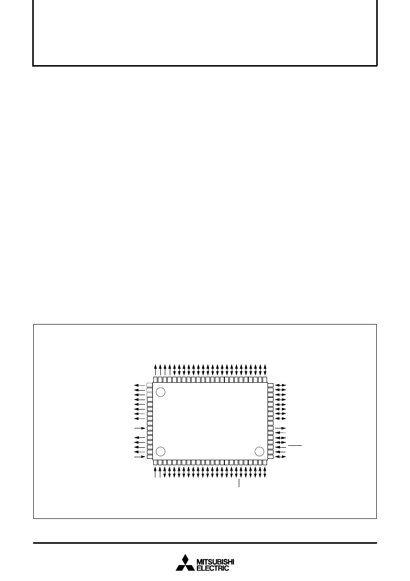
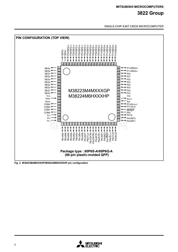
PIN CONFIGURATION (TOP VIEW)
SEG
8
SEG
9
SEG
10
SEG
11
P3
4
/SEG
12
P3
5
/SEG
13
P3
6
/SEG
14
P3
7
/SEG
15
P0
0
/SEG
16
P0
1
/SEG
17
P0
2
/SEG
18
P0
3
/SEG
19
P0
4
/SEG
20
P0
5
/SEG
21
P0
6
/SEG
22
P0
7
/SEG
23
P1
0
/SEG
24
P1
1
/SEG
25
P1
2
/SEG
26
P1
3
/SEG
27
P1
4
/SEG
28
P1
5
/SEG
29
P1
6
/SEG
30
P1
7
/SEG
31
64 63 62 61 60 59 58 57 56 55 54 53 52 51 50 49 48 47 46 45 44 43 42 41
SEG
7
SEG
6
SEG
5
SEG
4
SEG
3
SEG
2
SEG
1
SEG
0
V
CC
V
REF
AV
SS
COM
3
COM
2
COM
1
COM
0
VL
3
65
66
67
68
69
70
71
72
73
74
75
76
77
78
79
80
1 2 3 4 5 6 7 8 9 10 11 12 13 14 15 16 17 18 19 20 21 22 23 24
40
39
38
37
36
35
34
M38224M6HXXXFP
33
32
31
30
29
28
27
26
25
P2
0
P2
1
P2
2
P2
3
P2
4
P2
5
P2
6
P2
7
V
SS
X
OUT
X
IN
P7
0
/X
COUT
P7
1
/X
CIN
RESET
P4
0
P4
1
/蠁
Package type : 80P6N-A (80-pin plastic-molded QFP)
Fig. 1 M38224M6HXXXFP pin configuration
(The pin configuration of 80D0 is same as this.)
VL
2
VL
1
P6
7
/AN
7
P6
6
/AN
6
P6
5
/AN
5
P6
4
/AN
4
P6
3
/AN
3
P6
2
/AN
2
P6
1
/AN
1
P6
0
/AN
0
P5
7
/ADT
P5
6
/T
OUT
P5
5
/CNTR
1
P5
4
/CNTR
0
P5
3
/RTP
1
P5
2
/RTP
0
P5
1
/INT
3
P5
0
/INT
2
P4
7
/S
RDY
P4
6
/S
CLK
P4
5
/T
X
D
P4
4
/R
X
D
P4
3
/INT
1
P4
2
/INT
0


 1
1
 2
2
 3
3
 4
4
 5
5
 6
6
 7
7
 8
8
 9
9
 10
10
 11
11
 12
12
 13
13
 14
14
 15
15
 16
16
 17
17
 18
18
 19
19
 20
20
 21
21
 22
22
 23
23
 24
24
 25
25
 26
26
 27
27
 28
28
 29
29
 30
30
 31
31
 32
32
 33
33
 34
34
 35
35
 36
36
 37
37
 38
38
 39
39
 40
40
 41
41
 42
42
 43
43
 44
44
 45
45
 46
46
 47
47
 48
48
 49
49
 50
50
 51
51
 52
52
 53
53
 54
54
 55
55
 56
56
 57
57
 58
58
 59
59
 60
60
 61
61
 62
62
 63
63
 64
64
 65
65
 66
66
 67
67
 68
68
 69
69
 70
70
 71
71
 72
72
 73
73
 74
74
 75
75
 76
76
 77
77
 78
78
