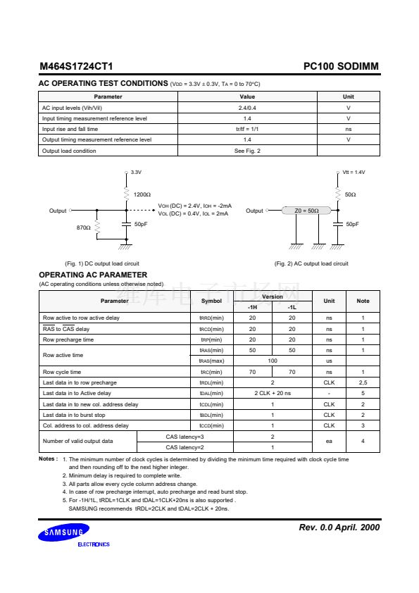
鈥?/div>
Max Freq. (Speed)
100MHz (10ns @ CL=2)
100MHz (10ns @ CL=3)
Burst mode operation
Auto & self refresh capability (4096 Cycles/64ms)
LVTTL compatible inputs and outputs
Single 3.3V
卤
0.3V power supply
MRS cycle with address key programs
Latency (Access from column address)
Burst length (1, 2, 4, 8 & Full page)
Data scramble (Sequential & Interleave)
鈥?All inputs are sampled at the positive going edge of the
system clock
鈥?Serial presence detect with EEPROM
鈥?PCB :
Height (1,250mil)
, double sided component
PIN CONFIGURATIONS (Front side/back side)
Pin Front Pin
1
3
5
7
9
11
13
15
17
19
21
23
25
27
29
31
33
35
37
39
41
43
45
47
49
V
SS
DQ0
DQ1
DQ2
DQ3
V
DD
DQ4
DQ5
DQ6
DQ7
V
SS
DQM0
DQM1
V
DD
A0
A1
A2
V
SS
DQ8
DQ9
DQ10
DQ11
V
DD
DQ12
DQ13
2
4
6
8
10
12
14
16
18
20
22
24
26
28
30
32
34
36
38
40
42
44
46
48
50
Back
V
SS
DQ32
DQ33
DQ34
DQ35
V
DD
DQ36
DQ37
DQ38
DQ39
V
SS
DQM4
DQM5
V
DD
A3
A4
A5
V
SS
DQ40
DQ41
DQ42
DQ43
V
DD
DQ44
DQ45
Pin Front
51
53
55
57
59
DQ14
DQ15
V
SS
NC
NC
Pin
52
54
56
58
60
Back
Pin
Front
DQ21
DQ22
DQ23
V
DD
A6
A8
V
SS
A9
A10/AP
V
DD
DQM2
DQM3
V
SS
DQ24
DQ25
DQ26
DQ27
V
DD
DQ28
DQ29
DQ30
DQ31
V
SS
**SDA
V
DD
Pin
96
98
100
102
104
106
108
110
112
114
116
118
120
122
124
126
128
130
132
134
136
138
140
142
144
Back
DQ53
DQ54
DQ55
V
DD
A7
BA0
V
SS
BA1
A11
V
DD
DQM6
DQM7
V
SS
DQ56
DQ57
DQ58
DQ59
V
DD
DQ60
DQ61
DQ62
DQ63
V
SS
**SCL
V
DD
DQ46 95
DQ47 97
V
SS
99
NC
101
NC
103
105
107
Voltage Key
109
CLK0 62 CKE0 111
V
DD
64
V
DD
113
RAS 66 CAS 115
WE
68 CKE1 117
CS0
70 *A12 119
CS1
72 *A13 121
DU
74 CLK1 123
V
SS
76
V
SS
125
NC
78
NC
127
NC
80
NC
129
V
DD
82
V
DD
131
DQ16 84 DQ48 133
DQ17 86 DQ49 135
DQ18 88 DQ50 137
DQ19 90 DQ51 139
V
SS
92
V
SS
141
DQ20 94 DQ52 143
PIN NAMES
Pin Name
A0 ~ A11
BA0 ~ BA1
DQ0 ~ DQ63
CLK0 ~ CLK1
CS0 ~ CS1
RAS
CAS
WE
DQM0 ~ 7
V
DD
V
SS
SDA
SCL
DU
NC
Function
Address input (Multiplexed)
Select bank
Data input/output
Clock input
Chip select input
Row address strobe
Column address strobe
Write enable
DQM
Power supply (3.3V)
Ground
Serial data I/O
Serial clock
Don鈥瞭 use
No connection
CKE0 ~ CKE1 Clock enable input
61
63
65
67
69
71
73
75
77
79
81
83
85
87
89
91
93
* These pins are not used in this module.
**
These pins should be NC in the system
which does not support SPD.
* SAMSUNG ELECTRONICS CO., Ltd. reserves the right to change products and specifications without notice.
Rev. 0.0 April. 2000


 1
1
 2
2
 3
3
 4
4
 5
5
 6
6
 7
7
 8
8
 9
9
