鈻?/div>
SUPPLY VOLTAGE
鈥?V
CC
= 3 V to 3.6 V for Program, Erase and
Read Operations
鈥?V
PP
= 12 V for Fast Program and Fast
Erase
TWO INTERFACES
鈥?Firmware Hub (FWH) Interface for
embedded operation with PC Chipsets
鈥?Address/Address Multiplexed (A/A Mux)
Interface for programming equipment
compatibility
FIRMWARE HUB (FWH) HARDWARE
INTERFACE MODE
鈥?5 Signal Communication Interface
supporting Read and Write Operations
鈥?Hardware Write Protect Pins for Block
Protection
鈥?Register Based Read and Write
Protection
鈥?5 Additional General Purpose Inputs for
platform design flexibility
鈥?Multi-byte Read Operation (4/16/128-
byte)
鈥?Synchronized with 33 MHz PCI clock
BYTE PROGRAMMING TIME
鈥?Single Byte Mode: 10碌s (typical)
鈥?Quadruple Byte Mode: 2.5碌s (typical)
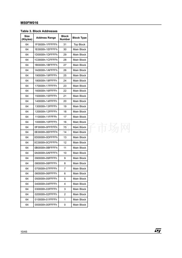
32 UNIFORM 64 Kbyte MEMORY BLOCKS
PROGRAM and ERASE SUSPEND
鈥?Read other Blocks during Program/Erase
Suspend
鈥?Program other Blocks during Erase
Suspend
FOR USE in PC BIOS APPLICATIONS
ELECTRONIC SIGNATURE
鈥?Manufacturer Code: 20h
鈥?Device Code: 2Eh
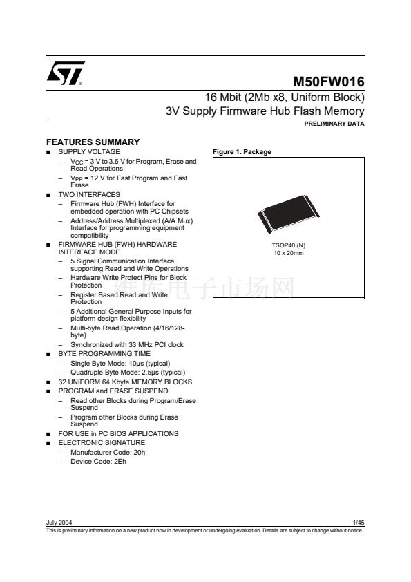
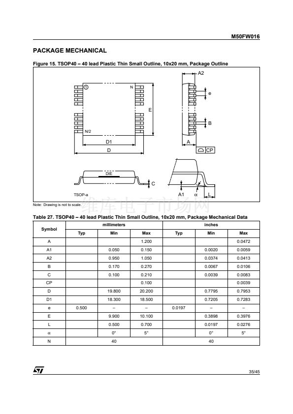
Figure 1. Package
TSOP40 (N)
10 x 20mm
July 2004
1/45
This is preliminary information on a new product now in development or undergoing evaluation. Details are subject to change without notice.


 1
1
 2
2
 3
3
 4
4
 5
5
 6
6
 7
7
 8
8
 9
9
 10
10
 11
11
 12
12
 13
13
 14
14
 15
15
 16
16
 17
17
 18
18
 19
19
 20
20
 21
21
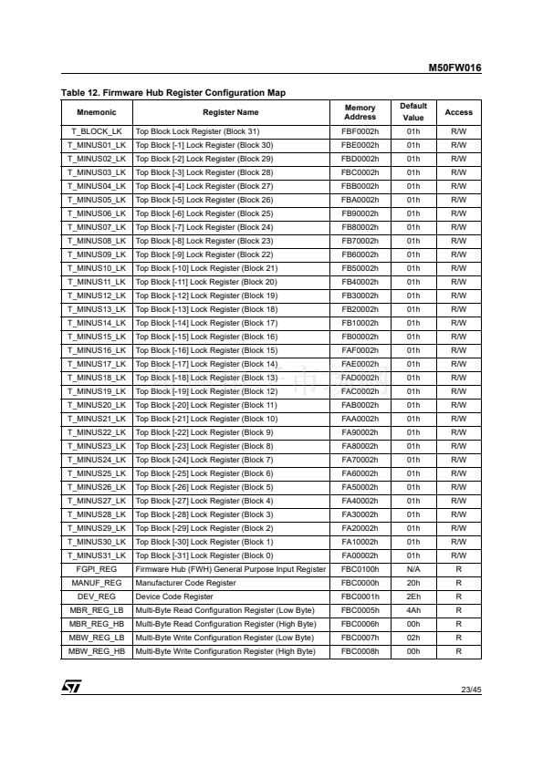
 22
22
 23
23
 24
24
 25
25
 26
26
 27
27
 28
28
 29
29
 30
30
 31
31
 32
32
 33
33
 34
34
 35
35
 36
36
 37
37
 38
38
 39
39
 40
40
 41
41
 42
42
 43
43
 44
44
 45
45
