鈥?/div>
High Speed: t
PD
= 3.6 ns (Typ) at V
CC
= 5.0 V
Low Power Dissipation: I
CC
= 1.0
mA
(Max) at T
A
= 25掳C
Power Down Protection Provided on Inputs
Balanced Propagation Delays
Pin and Function Compatible with Other Standard Logic Families
Chip Complexity: FETs = 68; Equivalent Gates = 16
Pb鈭扚ree Packages are Available
VD
= Device Code
M
= Date Code*
A
= Assembly Location
Y
= Year
W
= Work Week
G
= Pb鈭扚ree Package
(Note: Microdot may be in either location)
*Date Code orientation and/or position may
vary depending upon manufacturing location.
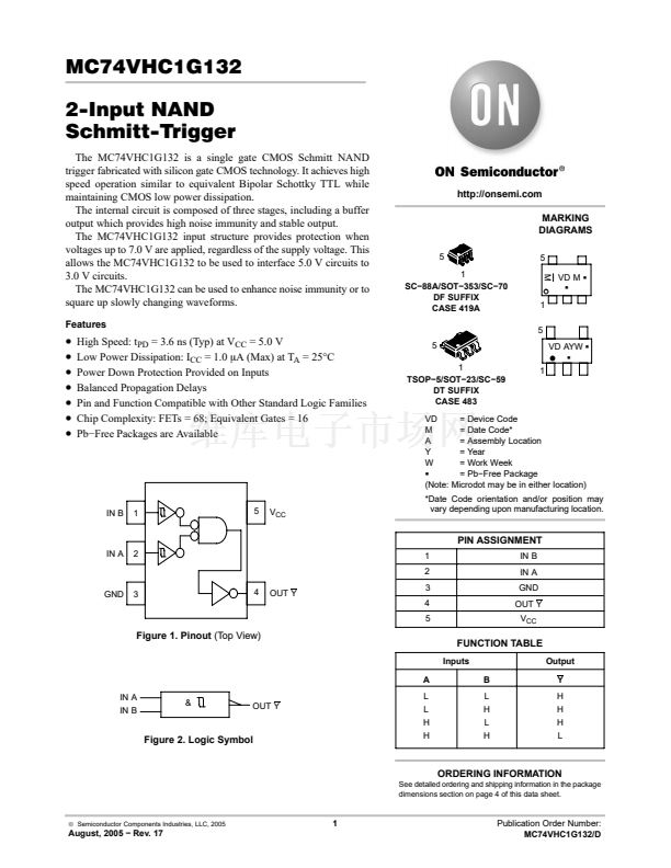
IN B
1
5
V
CC
PIN ASSIGNMENT
IN A
2
1
2
GND
3
4
OUT Y
3
4
5
IN B
IN A
GND
OUT Y
V
CC
Figure 1. Pinout
(Top View)
FUNCTION TABLE
Inputs
A
B
L
H
L
H
Output
Y
H
H
H
L
IN A
IN B
&
OUT Y
Figure 2. Logic Symbol
L
L
H
H
ORDERING INFORMATION
See detailed ordering and shipping information in the package
dimensions section on page 4 of this data sheet.
漏
Semiconductor Components Industries, LLC, 2005
1
August, 2005 鈭?Rev. 17
Publication Order Number:
MC74VHC1G132/D


 1
1
 2
2
 3
3
 4
4
 5
5
 6
6
