鈮?/div>
10
msec,
T
C
= 93掳C)
Operating Junction Temperature Range
Storage Temperature Range
Symbol
V
DRM,
V
RRM
I
T(RMS)
Value
600
YWW
AC
4DLM
4.0
A
4
I
TSM
I
2
t
P
GM
P
G(AV)
I
GM
V
GM
T
J
T
stg
40
6.6
0.5
0.1
0.2
5.0
鈭?0 to
110
鈭?0 to
150
A
A
2
sec
W
W
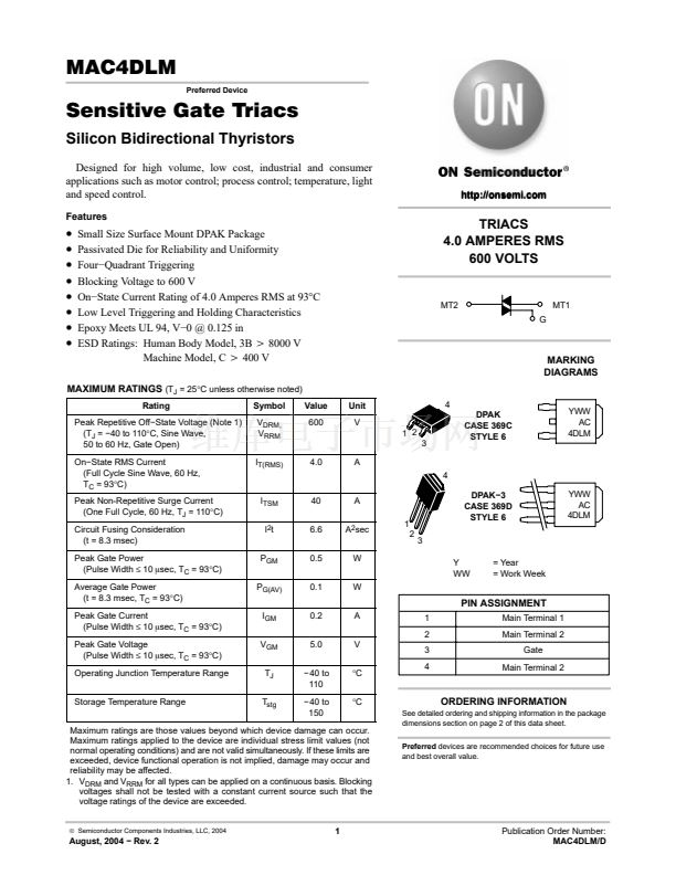
1
2
3
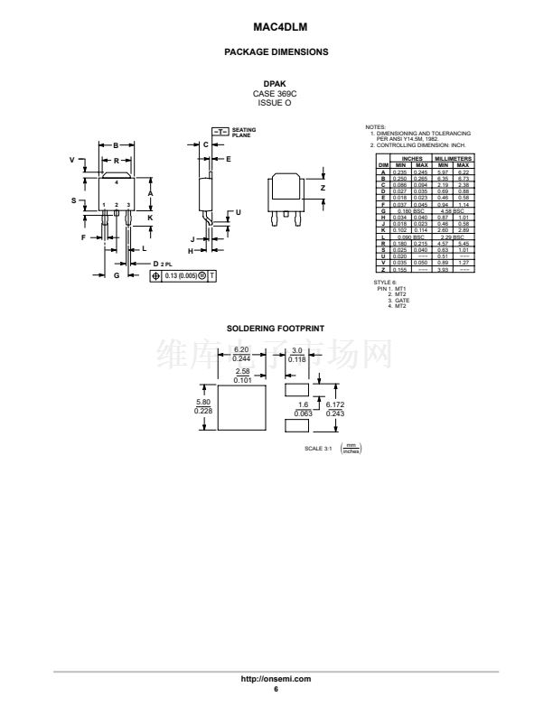
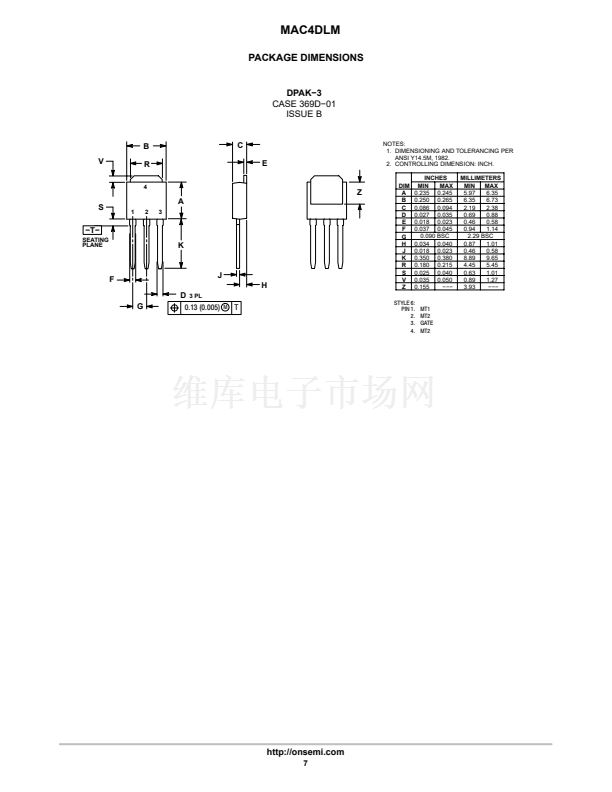
DPAK鈭?
CASE 369D
STYLE 6
YWW
AC
4DLM
Y
WW
= Year
= Work Week
PIN ASSIGNMENT
A
V
掳C
掳C
1
2
3
4
Main Terminal 1
Main Terminal 2
Gate
Main Terminal 2
ORDERING INFORMATION
See detailed ordering and shipping information in the package
dimensions section on page 2 of this data sheet.
Preferred
devices are recommended choices for future use
and best overall value.
Maximum ratings are those values beyond which device damage can occur.
Maximum ratings applied to the device are individual stress limit values (not
normal operating conditions) and are not valid simultaneously. If these limits are
exceeded, device functional operation is not implied, damage may occur and
reliability may be affected.
1. V
DRM
and V
RRM
for all types can be applied on a continuous basis. Blocking
voltages shall not be tested with a constant current source such that the
voltage ratings of the device are exceeded.
漏
Semiconductor Components Industries, LLC, 2004
1
August, 2004 鈭?Rev. 2
Publication Order Number:
MAC4DLM/D


 1
1
 2
2
 3
3
 4
4
 5
5
 6
6
 7
7
 8
8
