MC100LVEL14
3.3V ECL 1:5 Clock
Distribution Chip
Description
The MC100LVEL14 is a low skew 1:5 clock distribution chip
designed explicitly for low skew clock distribution applications. The
device can be driven by either a differential or single-ended ECL or, if
positive power supplies are used, PECL input signal. The LVEL14 is
functionally and pin compatible with the EL14 but is designed to
operate in ECL or PECL mode for a voltage supply range of
鈭?.0
V to
鈭?.8
V ( or 3.0 V to 3.8 V).
The LVEL14 features a multiplexed clock input to allow for the
distribution of a lower speed scan or test clock along with the high speed
system clock. When LOW (or left open and pulled LOW by the input
pulldown resistor) the SEL pin will select the differential clock input.
The common enable (EN) is synchronous so that the outputs will only
be enabled/disabled when they are already in the LOW state. This
avoids any chance of generating a runt clock pulse when the device is
enabled/disabled as can happen with an asynchronous control. The
internal flip flop is clocked on the falling edge of the input clock,
therefore all associated specification limits are referenced to the
negative edge of the clock input.
The V
BB
pin, an internally generated voltage supply, is available to
this device only. For single鈭抏nded input conditions, the unused
differential input is connected to V
BB
as a switching reference voltage.
V
BB
may also rebias AC coupled inputs. When used, decouple V
BB
and
V
CC
via a 0.01
mF
capacitor and limit current sourcing or sinking to 0.5
mA. When not used, V
BB
should be left open.
Features
http://onsemi.com
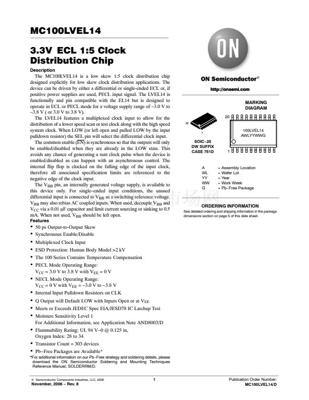
MARKING
DIAGRAM
20
20
1
100LVEL14
AWLYYWWG
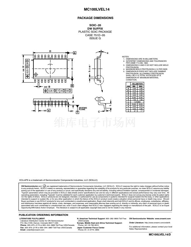
SOIC鈭?0
DW SUFFIX
CASE 751D
1
A
WL
YY
WW
G
= Assembly Location
= Wafer Lot
= Year
= Work Week
= Pb鈭扚ree Package
ORDERING INFORMATION
See detailed ordering and shipping information in the package
dimensions section on page 5 of this data sheet.
鈥?/div>
鈥?/div>
鈥?/div>
鈥?/div>
鈥?/div>
鈥?/div>
50 ps Output-to-Output Skew
Synchronous Enable/Disable
Multiplexed Clock Input
ESD Protection: Human Body Model >2 kV
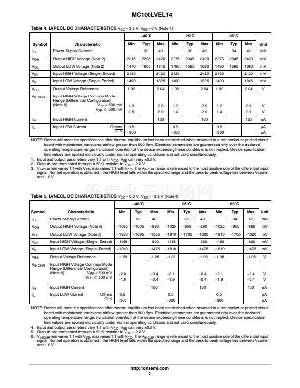
The 100 Series Contains Temperature Compensation
PECL Mode Operating Range:
V
CC
= 3.0 V to 3.8 V with V
EE
= 0 V
鈥?/div>
NECL Mode Operating Range:
V
CC
= 0 V with V
EE
=
鈭?.0
V to
鈭?.8
V
鈥?/div>
Internal Input Pulldown Resistors on CLK
鈥?/div>
Q Output will Default LOW with Inputs Open or at V
EE
鈥?/div>
Meets or Exceeds JEDEC Spec EIA/JESD78 IC Latchup Test
鈥?/div>
Moisture Sensitivity Level 1
For Additional Information, see Application Note AND8003/D
鈥?/div>
Flammability Rating: UL 94 V鈭? @ 0.125 in,
Oxygen Index: 28 to 34
鈥?/div>
Transistor Count = 303 devices
鈥?/div>
Pb鈭扚ree Packages are Available*
*For additional information on our Pb鈭扚ree strategy and soldering details, please
download the ON Semiconductor Soldering and Mounting Techniques
Reference Manual, SOLDERRM/D.
漏
Semiconductor Components Industries, LLC, 2006
November, 2006
鈭?/div>
Rev. 8
1
Publication Order Number:
MC100LVEL14/D
MC100LVEL14_06 PDF文件相关型号
MC100LVEL14DWG,MC100LVEL14DWR2,MC100LVEL14DWR2G
MC100LVEL14_06相关型号PDF文件下载


 1
1
 2
2
 3
3
 4
4
 5
5
 6
6
