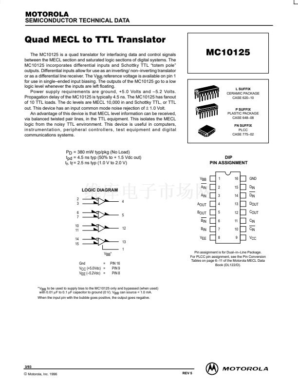
between the MECL section and saturated logic sections of digital systems. The
MC10125 incorporates differential inputs and Schottky TTL 鈥渢otem pole鈥?/div>
outputs. Differential inputs allow for use as an inverting/ non鈥搃nverting translator
or as a differential line receiver. The VBB reference voltage is available on pin 1
for use in single鈥揺nded input biasing. The outputs of the MC10125 go to a low
logic level whenever the inputs are left floating.
Power supply requirements are ground, +5.0 Volts and 鈥?.2 Volts.
Propagation delay of the MC10125 is typically 4.5 ns. The MC10125 has fanout
of 10 TTL loads. The dc levels are MECL 10,000 in and Schottky TTL, or TTL
out. This device has an input common mode noise rejection of
卤
1.0 Volt.
An advantage of this device is that MECL level information can be received,
via balanced twisted pair lines, in the TTL equipment. This isolates the MECL
logic from the noisy TTL environment. This device is useful in computers,
instrumentation, peripheral controllers, test equipment and digital
communications systems.
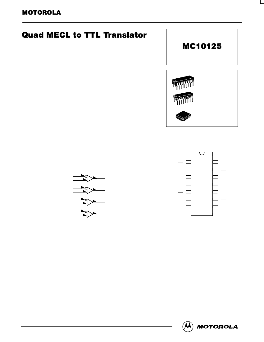
MC10125
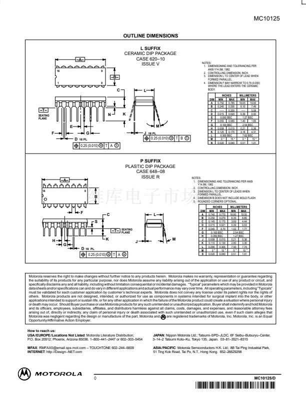
L SUFFIX
CERAMIC PACKAGE
CASE 620鈥?0
P SUFFIX
PLASTIC PACKAGE
CASE 648鈥?8
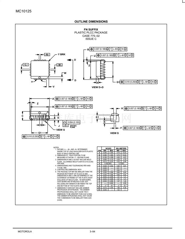
FN SUFFIX
PLCC
CASE 775鈥?2
PD = 380 mW typ/pkg (No Load)
tpd = 4.5 ns typ (50% to + 1.5 Vdc out)
tr, tf = 2.5 ns typ (1.0 V to 2.0 V)
VBB
DIP
PIN ASSIGNMENT
1
2
3
4
5
6
7
8
16
15
14
13
12
11
10
9
GND
DIN
DIN
DOUT
COUT
CIN
CIN
VCC
LOGIC DIAGRAM
2
3
6
7
10
11
14
15
VBB*
Gnd
=
VCC (+5.0Vdc) =
VEE (鈥?.2Vdc) =
PIN 16
PIN 9
PIN 8
4
AIN
AIN
AOUT
BOUT
BIN
12
BIN
VEE
5
13
1
Pin assignment is for Dual鈥搃n鈥揕ine Package.
For PLCC pin assignment, see the Pin Conversion
Tables on page 6鈥?1 of the Motorola MECL Data
Book (DL122/D).
* VBB to be used to supply bias to the MC10125 only and bypassed (when used)
with 0.01
碌F
to 0.1
碌F
capacitor to ground (0 V). VBB can source < 1.0 mA.
When the input pin with the bubble goes positive, the output goes negative.
3/93
漏
Motorola, Inc. 1996
3鈥?9
REV 5


 1
1
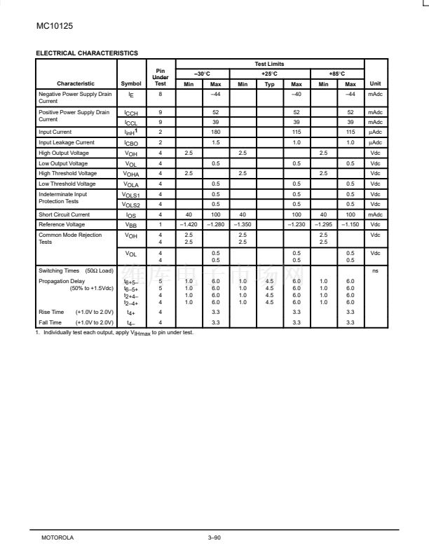 2
2
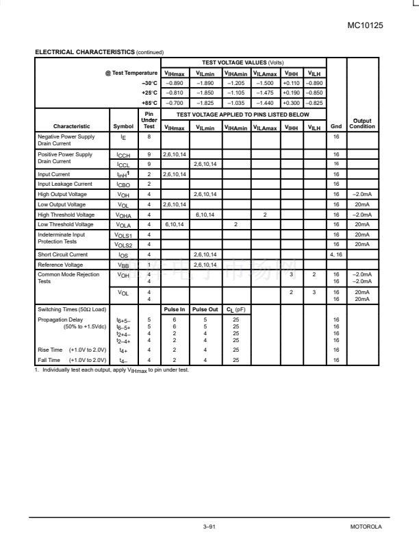 3
3
 4
4
 5
5
 6
6
 7
7
