鈥?/div>
Pb鈭扚ree Packages are Available*
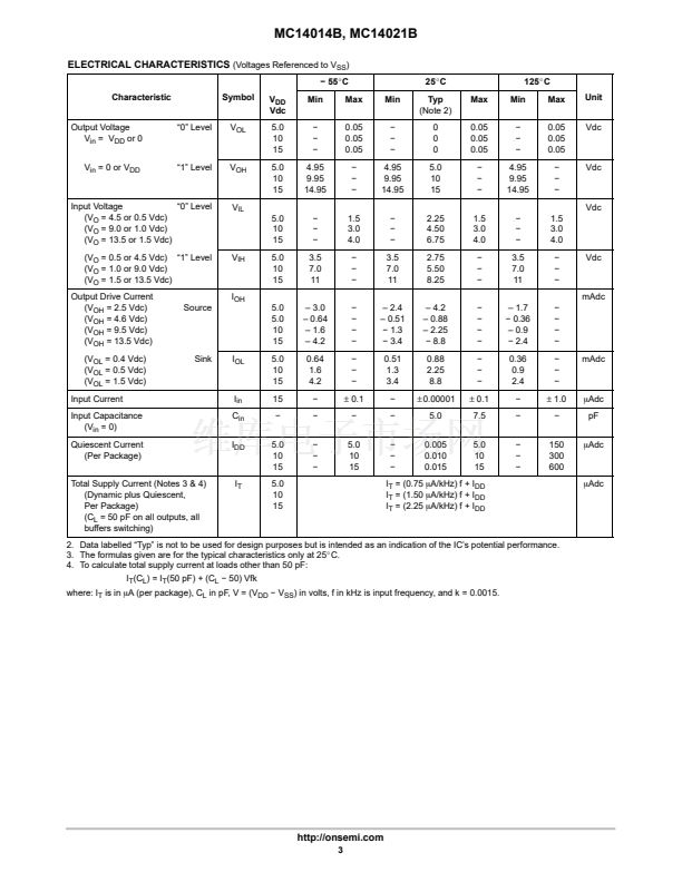
MAXIMUM RATINGS
(Voltages Referenced to V
SS
)
Symbol
V
DD
V
in
, V
out
I
in
, I
out
P
D
T
A
T
stg
T
L
Parameter
DC Supply Voltage Range
Input or Output Voltage Range
(DC or Transient)
Input or Output Current
(DC or Transient) per Pin
Power Dissipation, per Package
(Note 1)
Ambient Temperature Range
Storage Temperature Range
Lead Temperature
(8鈭扴econd Soldering)
Value
鈭?.5 to +18.0
鈭?.5 to V
DD
+ 0.5
卤
10
500
鈭?5 to +125
鈭?5 to +150
260
Unit
V
V
mA
mW
掳C
掳C
掳C
xx
A
WL, L
YY, Y
WW, W
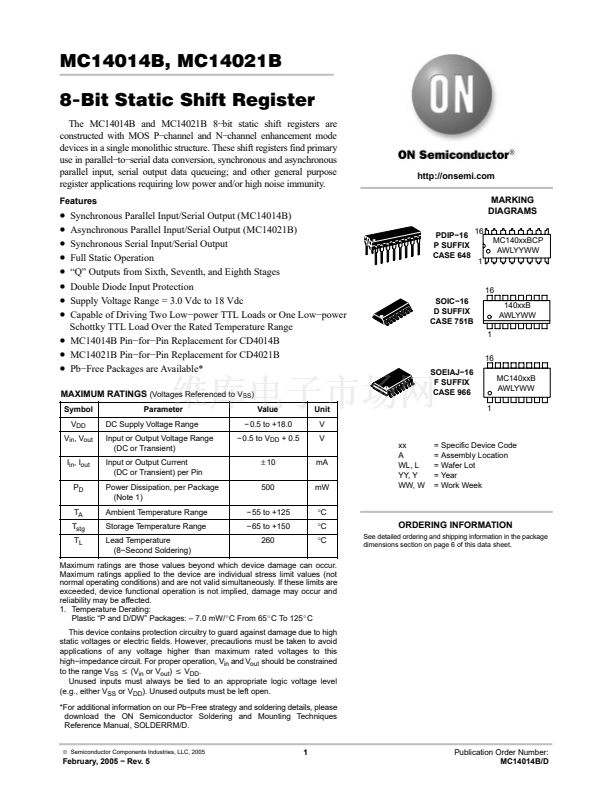
16
SOIC鈭?6
D SUFFIX
CASE 751B
1
16
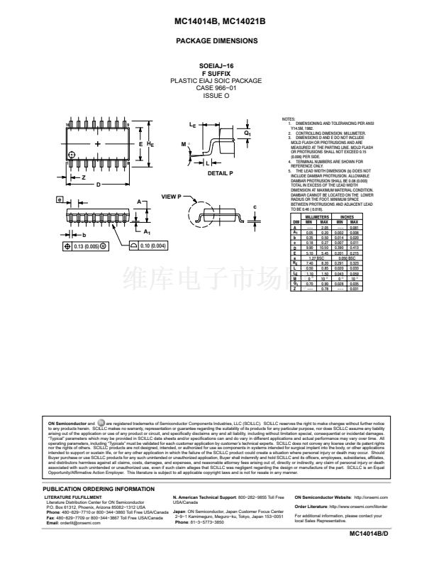
SOEIAJ鈭?6
F SUFFIX
CASE 966
1
MC140xxB
AWLYWW
140xxB
AWLYWW
= Specific Device Code
= Assembly Location
= Wafer Lot
= Year
= Work Week
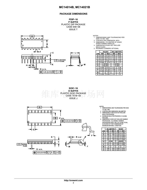
ORDERING INFORMATION
See detailed ordering and shipping information in the package
dimensions section on page 6 of this data sheet.
Maximum ratings are those values beyond which device damage can occur.
Maximum ratings applied to the device are individual stress limit values (not
normal operating conditions) and are not valid simultaneously. If these limits are
exceeded, device functional operation is not implied, damage may occur and
reliability may be affected.
1. Temperature Derating:
Plastic 鈥淧 and D/DW鈥?Packages: 鈥?7.0 mW/_C From 65_C To 125_C
This device contains protection circuitry to guard against damage due to high
static voltages or electric fields. However, precautions must be taken to avoid
applications of any voltage higher than maximum rated voltages to this
high鈭抜mpedance circuit. For proper operation, V
in
and V
out
should be constrained
to the range V
SS
v
(V
in
or V
out
)
v
V
DD
.
Unused inputs must always be tied to an appropriate logic voltage level
(e.g., either V
SS
or V
DD
). Unused outputs must be left open.
*For additional information on our Pb鈭扚ree strategy and soldering details, please
download the ON Semiconductor Soldering and Mounting Techniques
Reference Manual, SOLDERRM/D.
漏
Semiconductor Components Industries, LLC, 2005
1
February, 2005 鈭?Rev. 5
Publication Order Number:
MC14014B/D


 1
1
 2
2
 3
3
 4
4
 5
5
 6
6
 7
7
 8
8
